Archive for October, 2014
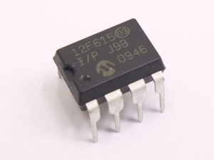
 Break IC PIC12F615 Software
Break IC PIC12F615 Software
Break IC PIC12F615 Software from its memory, it is important to know the basic features of PIC12F615 and then disable its protection mechanism:
High-Performance RISC CPU:
· Only 35 instructions to learn:
– All single-cycle instructions except branches
· Operating speed:
– DC – 20 MHz oscillator/clock input
– DC – 200 ns instruction cycle
· Interrupt capability
· 8-level deep hardware stack
· Direct, Indirect and Relative Addressing modes
Special Microcontroller Features:
· Precision Internal Oscillator:
– Factory calibrated to ±1%, typical
– Software selectable frequency: 4 MHz or 8 MHz
· Power-Saving Sleep mode
· Voltage range:
– PIC12F609/615: 2.0V to 5.5V
– PIC12HV609/615: 2.0V to user defined maximum (see note)
· Industrial and Extended Temperature range
· Power-on Reset (POR)
· Power-up Timer (PWRT) and Oscillator Start-up Timer (OST)
· Brown-out Reset (BOR)
· Watchdog Timer (WDT) with independent oscillator for reliable operation
· Multiplexed Master Clear with pull-up/input pin
· Programmable code protection
· High Endurance Flash:
– 100,000 write Flash endurance
– Flash retention: > 40 years
Break IC PIC12F615 Software
Low-Power Features:
· Standby Current:
– 50 nA @ 2.0V, typical
· Operating Current:
– 11 ìA @ 32 kHz, 2.0V, typical
– 260 ìA @ 4 MHz, 2.0V, typical
· Watchdog Timer Current:
– 1 ìA @ 2.0V, typical
Peripheral Features:
· Shunt Voltage Regulator (PIC12HV609/615 only)
– 5 volt regulation
– 4 mA to 50 mA shunt range
· 5 I/O pins and 1 input only
· High current source/sink for direct LED drive
– Interrupt-on-pin change or pins
– Individually programmable weak pull-ups
· Analog Comparator module with:
– One analog comparator
– Programmable on-chip voltage reference (CVREF) module (% of VDD)
– Comparator inputs and output externally accessible
– Built-In Hysteresis (software selectable)
· Timer0: 8-bit timer/counter with 8-bit programmable prescaler
· Enhanced Timer1:
– 16-bit timer/counter with prescaler
– External Timer1 Gate (count enable)
– Option to use OSC1 and OSC2 in LP mode as Timer1 oscillator if INTOSC mode selected
– Option to use system clock as Timer1
· In-Circuit Serial ProgrammingTM (ICSPTM) via two pins
PIC12F615/HV615 ONLY:
· Enhanced Capture, Compare, PWM module:
– 16-bit Capture, max. resolution 12.5 ns
– Compare, max. resolution 200 ns
– 10-bit PWM with 1 or 2 output channels, 1 output channel programmable “dead time”, max. frequency 20 kHz, auto-shutdown
· A/D Converter:
– 10-bit resolution and 4 channels, samples internal voltage references
· Timer2: 8-bit timer/counter with 8-bit period register, prescaler and postscaler
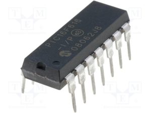
Break IC PIC16F616 Heximal
Break IC PIC16F616 Heximal
Break IC PIC16F616 Heximal from the program memory, below we will introduce the program memory organization chart so you can have a better idea about how to get access to the wafer die:
PIC16F616/16HV616 only:
· A/D Converter:
– 10-bit resolution
– 8 external input channels
– 2 internal reference channels
· Timer2: 8-bit timer/counter with 8-bit period register, prescaler and postscaler
· Enhanced Capture, Compare, PWM module:
– 16-bit Capture, max. resolution 12.5 ns
– 16-bit Compare, max. resolution 200 ns
– 10-bit PWM with 1, 2 or 4 output channels, programmable “dead time”, max. frequency 20 kHz
Program Memory Organization of PIC16F616/16HV616
The PIC16F610/616/16HV610/616 has a 13-bit program counter capable of addressing an 8k x 14 program memory space. Only the first 1K x 14 (0000h-3FF) for the PIC16F610/16HV610 and the first 2K x 14 (0000h-07FFh) for the PIC16F616/16HV616 is physically implemented. Accessing a location above these boundaries will cause a wraparound within the first 1K x 14 space (PIC16F610/16HV610) and 2K x 14 space (PIC16F616/16HV616). The Reset vector is at 0000h and the interrupt vector is at 0004h.
Break IC PIC16F616 Heximal
The data memory (see Figure 2-4) is partitioned into two banks, which contain the General Purpose Registers (GPR) and the Special Function Registers (SFR). The Special Function Registers are located in the first 32 locations of each bank.
PIC16F610/16HV610 Register locations 40h-7Fh in Bank 0 are General Purpose Registers, implemented PC gram counter capable of addressing an 8k x 14 program memory space. Only the first 1K x 14 (0000h-3FF) for the PIC16F610/16HV610 and the first 2K x 14 (0000h-07FFh) for the PIC16F616/16HV616 is physically implemented.
Accessing a location above these boundaries will cause a wraparound within the first 1K x 14 space (PIC16F610/16HV610) and 2K x 14 space (PIC16F616/16HV616). The Reset vector is at 0000h and the interrupt vector is at 0004h.