Archive for May, 2014
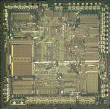
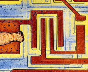
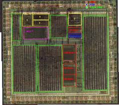
 Attack IC PIC18LF4520 Program
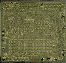
Attack IC PIC18LF4520 Program
Attack IC PIC18LF4520 protective memory, cut off the security fuse of the memory and extract Program and data from the flash and eeprom, Clone the content to other new Microcontroller PIC18LF4520 for the same functions;
Power Management Features:
Peripheral Highlights (Continued):
Run: CPU on, Peripherals on
Idle: CPU off, Peripherals on
Sleep: CPU off, Peripherals off
Ultra Low 50nA Input Leakage
Run mode Currents Down to 11 ìA Typical
Idle mode Currents Down to 2.5 ìA Typical
Sleep mode Current Down to 100 nA Typical
Timer1 Oscillator: 900 nA, 32 kHz, 2V
Watchdog Timer: 1.4 ìA, 2V Typical
Two-Speed Oscillator Start-up
· Master Synchronous Serial Port (MSSP) module
Supporting 3-Wire SPI (all 4 modes) and I2C™ Master and Slave modes
· Enhanced Addressable USART module:
– Supports RS-485, RS-232 and LIN/J2602
– RS-232 operation using internal oscillator
block (no external crystal required)
– Auto-wake-up on Start bit
– Auto-Baud Detect
· 10-Bit, up to 13-Channel Analog-to-Digital (A/D)
Flexible Oscillator Structure:
· Four Crystal modes, up to 40 MHz
· 4x Phase Lock Loop (PLL) – Available for Crystal and Internal Oscillators
· Two External RC modes, up to 4 MHz
· Two External Clock modes, up to 40 MHz
· Internal Oscillator Block:
– Fast wake from Sleep and Idle, 1 ìs typical
– 8 use-selectable frequencies, from 31 kHz to 8 MHz
– Provides a complete range of clock speeds from 31 kHz to 32 MHz when used with PLL
– User-tunable to compensate for frequency drift
· Secondary Oscillator using Timer1 @ 32 kHz
· Fail-Safe Clock Monitor:
– Allows for safe shutdown if peripheral clock stops
Peripheral Highlights:
Converter module:
– Auto-acquisition capability
– Conversion available during Sleep
· Dual Analog Comparators with Input Multiplexing
· Programmable 16-Level High/Low-Voltage Detection (HLVD) module:
– Supports interrupt on High/Low-Voltage Detection
Special Microcontroller Features:
· C Compiler Optimized Architecture:
– Optional extended instruction set designed to optimize re-entrant code
· 100,000 Erase/Write Cycle Enhanced Flash
Program Memory Typical
· 1,000,000 Erase/Write Cycle Data EEPROM
Memory Typical
· Flash/Data EEPROM Retention: 100 Years Typical
· Self-Programmable under Software Control
High-Current Sink/Source 25 mA/25 mA
Three Programmable External Interrupts
Four Input Change Interrupts
Up to 2 Capture/Compare/PWM (CCP) modules,
· Priority Levels for Interrupts
· 8 x 8 Single-Cycle Hardware Multiplier
· Extended Watchdog Timer (WDT):
– Programmable period from 4 ms to 131s one with Auto-Shutdown (28-pin devices)
· Enhanced Capture/Compare/PWM (ECCP) module (40/44-pin devices only):
– One, two or four PWM outputs
– Selectable polarity
– Programmable dead time
– Auto-shutdown and auto-restart
· Single-Supply 5V In-Circuit Serial
Programming™ (ICSP™) via Two Pins
· In-Circuit Debug (ICD) via Two Pins
· Wide Operating Voltage Range: 2.0V to 5.5V
· Programmable Brown-out Reset (BOR) with Software Enable Option
Break Chip SAF-C164CI-8EM Firmware
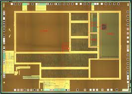
Break Chip SAF-C164CI-8EM Firmware
Break Chip SAF-C164CI-8EM encrypted memory and extract the Firmware out from its flash and eeprom memory, then copy the program and data to blank Microcontroller cloning;
16-Bit Single-Chip Microcontroller C164CI/SI, C164CL/SL
· High Performance 16-bit CPU with 4-Stage Pipeline
– 80 ns Instruction Cycle Time at 25 MHz CPU Clock
– 400 ns Multiplication (16 × 16 bit), 800 ns Division (32 / 16 bit)
– Enhanced Boolean Bit Manipulation Facilities
– Additional Instructions to Support HLL and Operating Systems
– Register-Based Design with Multiple Variable Register Banks
– Single-Cycle Context Switching Support
– 16 MBytes Total Linear Address Space for Code and Data
– 1024 Bytes On-Chip Special Function Register Area
· 16-Priority-Level Interrupt System with 32 Sources, Sample-Rate down to 40 ns
· 8-Channel Interrupt-Driven Single-Cycle Data Transfer Facilities via
Peripheral Event Controller (PEC)
· Clock Generation via on-chip PLL (factors 1:1.5/2/2.5/3/4/5) via prescaler or via direct clock input
· On-Chip Memory Modules
– 2 KBytes On-Chip Internal RAM (IRAM)
– 2 KBytes On-Chip Extension RAM (XRAM)
– up to 64 KBytes On-Chip Program Mask ROM or OTP Memory
· On-Chip Peripheral Modules
– 8-Channel 10-bit A/D Converter with Programmable Conversion Time down to 7.8 µs
– 8-Channel General Purpose Capture/Compare Unit (CAPCOM2)
– Capture/Compare Unit for flexible PWM Signal Generation (CAPCOM6) (3/6 Capture/Compare Channels and 1 Compare Channel)
– Multi-Functional General Purpose Timer Unit with 3 Timers
– Two Serial Channels (Synchronous/Asynchronous and High-Speed-Synchronous)
– On-Chip CAN Interface (Rev. 2.0B active) with 15 Message Objects (Full CAN/Basic CAN)
– On-Chip Real Time Clock
· Up to 4 MBytes External Address Space for Code and Data
– Programmable External Bus Characteristics for Different Address Ranges
– Multiplexed or Demultiplexed External Address/Data
– Four Optional Programmable Chip-Select Signals
· Idle, Sleep, and Power Down Modes with Flexible Power Management
· Programmable Watchdog Timer and Oscillator Watchdog
· Up to 59 General Purpose I/O Lines, partly with Selectable Input Thresholds and Hysteresis
· Supported by a Large Range of Development Tools like C-Compilers,
Macro-Assembler Packages, Emulators, Evaluation Boards, HLL-Debuggers,
Simulators, Logic Analyzer Disassemblers, Programming Boards
· On-Chip Bootstrap Loader
· 80-Pin MQFP Package, 0.65 mm pitch
This document describes several derivatives of the C164 group. Table 1 enumerates these derivatives and summarizes the differences. As this document refers to all of these derivatives, some descriptions may not apply to a specific product.
Break Microcontroller PIC12F629 Program
Break Microcontroller PIC12F629 Program
Break Microcontroller PIC12F629 locked memory and recover Program in the format of heximal from MCU by cracking MCU tamper resistance system and copy the code to blank MCU;
High-Performance RISC CPU:
· Only 35 Instructions to Learn
– All single-cycle instructions except branches
· Operating Speed:
– DC – 20 MHz oscillator/clock input when Break Microcontroller
– DC – 200 ns instruction cycle
· Interrupt Capability
· 8-Level Deep Hardware Stack
· Direct, Indirect, and Relative Addressing modes
Special Microcontroller Features:
· Internal and External Oscillator Options
– Precision Internal 4 MHz oscillator factory calibrated to ±1%
– External Oscillator support for crystals and resonators
– 5 ms wake-up from Sleep, 3.0V, typical
· Power-Saving Sleep mode
· Wide Operating Voltage Range – 2.0V to 5.5V
· Industrial and Extended Temperature Range
· Low-Power Power-on Reset (POR)
· Power-up Timer (PWRT) and Oscillator Start-up Timer (OST)
· Brown-out Detect (BOD)
· Watchdog Timer (WDT) with Independent Oscillator for Reliable Operation
· Multiplexed MCLR/Input Pin
· Interrupt-on-Pin Change
· Individual Programmable Weak Pull-ups
· Programmable Code Protection
· High Endurance Flash/EEPROM Cell
– 100,000 write Flash endurance
– 1,000,000 write EEPROM endurance
– Flash/Data EEPROM Retention: > 40 years
Low-Power Features:
· Standby Current:
– 1 nA @ 2.0V, typical
· Operating Current:
– 8.5 mA @ 32 kHz, 2.0V, typical
– 100 mA @ 1 MHz, 2.0V, typical
· Watchdog Timer Current
– 300 nA @ 2.0V, typical
· Timer1 Oscillator Current:
– 4 mA @ 32 kHz, 2.0V, typical
Peripheral Features:
· 6 I/O Pins with Individual Direction Control
· High Current Sink/Source for Direct LED Drive
· Analog Comparator module with:
– One analog comparator
– Programmable on-chip comparator voltage reference (CVREF) module
– Programmable input multiplexing from device inputs
– Comparator output is externally accessible
· Analog-to-Digital Converter module (PIC12F675):
– 10-bit resolution
– Programmable 4-channel input
– Voltage reference input
· Timer0: 8-Bit Timer/Counter with 8-Bit Programmable Prescaler
· Enhanced Timer1:
– 16-bit timer/counter with prescaler
– External Gate Input mode
– Option to use OSC1 and OSC2 in LP mode as Timer1 oscillator, if INTOSC mode selected
· In-Circuit Serial ProgrammingTM (ICSPTM) via two pins
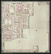
Break MCU dsPIC30F4011 Heximal
Break MCU dsPIC30F4011 Heximal
Break MCU dsPIC30F4011 memory and extract its Heximal out from its flash and eeprom, clone firmware to blank Microcontroller dsPIC30F4011 which will provide the same functions as original IC Clone;
Peripheral Features:
this group of dsPIC30F devices and is not intended to be a complete reference source. For more information on the CPU, peripherals, register descriptions and general device functionality, refer to the “dsPIC30F Family Reference Manual” (DS70046). For more information on the device instruction set and programming, refer to the “16-bit MCU and DSC Reference Manual” (DS70157).
High-Performance, Modified RISC CPU:
· Modified Harvard architecture
· C compiler optimized instruction set architecture with flexible addressing modes
· 83 base instructions
· 24-bit wide instructions, 16-bit wide data path
· 48 Kbytes on-chip Flash program space (16K instruction words)
· 2 Kbytes of on-chip data RAM
· 1 Kbyte of nonvolatile data EEPROM
· Up to 30 MIPS operation:
– DC to 40 MHz external clock input
– 4 MHz-10 MHz oscillator input with PLL active (4x, 8x, 16x)
· 30 interrupt sources:
– Three external interrupt sources
– Eight user-selectable priority levels for each
· High-current sink/source I/O pins: 25 mA/25 mA
· Timer module with programmable prescaler:
– Five 16-bit timers/counters; optionally pair 16-bit timers into 32-bit timer modules
· 16-bit Capture input functions
· 16-bit Compare/PWM output functions
· 3-wire SPI modules (supports 4 Frame modes)
· I2C™ module supports Multi-Master/Slave mode and 7-bit/10-bit addressing
· Two UART modules with FIFO Buffers
· CAN module, 2.0B compliant
Motor Control PWM Module Features:
· Six PWM output channels:
– Complementary or Independent Output modes
– Edge and Center-Aligned modes
· Three duty cycle generators
· Dedicated time base
· Programmable output polarity
· Dead-time control for Complementary mode
· Manual output control
· Trigger for A/D conversions
Quadrature Encoder Interface Module Features:
interrupt source
– Four processor trap sources
· 16 x 16-bit working register array
Phase A, Phase B and Index Pulse input 16-bit up/down position counter
Count direction status
Position Measurement (x2 and x4) mode
Programmable digital noise filters on inputs
Dual data fetch
Accumulator write-back for DSP operations
Alternate 16-bit Timer/Counter mode
Interrupt on position counter rollover/underflow
Modulo and Bit-Reversed Addressing modes
Two, 40-bit wide accumulators with optional saturation logic
Analog Features:
· 17-bit x 17-bit single-cycle hardware fractional/integer multiplier
· All DSP instructions are single cycle
· ±16-bit, single-cycle shift
· 10-bit Analog-to-Digital Converter (ADC) with four Sample and Holde (S&H) inputs:
– 1 Msps conversion rate
– Nine input channels
– Conversion available during Sleep and Idle
· Programmable Brown-out Reset only
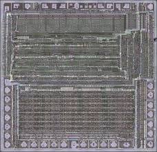
Break IC STM32F101C4T6TR Binary
Break IC STM32F101C4T6TR Binary
Break IC STM32F101C4T6TR memory and extract the binary or heximal out from the MCU flash and eeprom, duplicate the code to other new blank microcontroller STM32F101C4T6 which will provide the same functions;
Features
Core: ARM 32-bit Cortex™-M3 CPU
– 36 MHz maximum frequency, 1.25 DMIPS/MHz (Dhrystone 2.1) performance at 0 wait state memory
– Single-cycle multiplication and hardware division Up to 5 timers
– Up to two16-bit timers, each with up to 4 Memories
– 16 to 32 Kbytes of Flash memory
– 4 to 6 Kbytes of SRAM Clock, reset and supply management IC/OC/PWM or pulse counter
– 2 watchdog timers (Independent and Window)
– SysTick timer: 24-bit downcounter
– 2.0 to 3.6 V application supply and I/Os
– POR, PDR and programmable voltage detector (PVD)
– 4-to-16 MHz crystal oscillator
– Internal 8 MHz factory-trimmed RC
– Internal 40 kHz RC
– PLL for CPU clock
– 32 kHz oscillator for RTC with calibration Up to 4 communication interfaces
– 1 x I2C interface (SMBus/PMBus)
– Up to 2 USARTs (ISO 7816 interface, LIN, IrDA capability, modem control)
– 1 × SPI (18 Mbit/s) CRC calculation unit, 96-bit unique ID
Device summary
– Sleep, Stop and Standby modes
– VBAT supply for RTC and backup registers
Reference
Part number
STM32F101C4, Debug mode
– Serial wire debug (SWD) and JTAG interfaces DMA
STM32F101x4
STM32F101x6
STM32F101R4,
STM32F101T4
STM32F101C6,
STM32F101R6,
STM32F101T6
– 7-channel DMA controller
– Peripherals supported: timers, ADC, SPIs, I2Cs and USARTs 1 × 12-bit, 1 µs A/D converter (up to 16 channels)
– Conversion range: 0 to 3.6 V
– Temperature sensor Up to 51 fast I/O ports
– 26/37/51 I/Os, all mappable on 16 external interrupt vectors and almost all 5 V-tolerant
Recover Chip C8051F340 Firmware
Recover Chip C8051F340 Firmware
Recover Chip C8051F340 Firmware include the program from flash and data from eeprom memory through MCU Cracking technique, then replicate the content to other blank Microcontroller C8051F340;
Analog Peripherals
High Speed 8051 µC Core 10-Bit ADC (C8051F340/1/2/3/4/5/6/7/A/B only)
Pipelined instruction architecture; executes 70% of Up to 200 ksps
Built-in analog multiplexer with single-ended and differential mode
VREF from external pin, internal reference, or VDD
Instructions in 1 or 2 system clocks 48 MIPS and 25 MIPS versions available.
Expanded interrupt handler
· Built-in temperature sensor
· External conversion start input option
Two comparators Internal voltage reference
Memory
– 4352 or 2304 Bytes RAM
– 64 or 32 kB Flash; In-system programmable in 512-byte
(C8051F340/1/2/3/4/5/6/7/A/B only)
– Brown-out detector and POR Circuitry
USB Function Controller
– USB specification 2.0 compliant
– Full speed (12 Mbps) or low speed (1.5 Mbps) operation sectors
Digital Peripherals
– 40/25 Port I/O; All 5 V tolerant with high sink current
– Hardware enhanced SPI™, SMBus™, and one or two enhanced UART serial ports
Integrated clock recovery; no external crystal required for full speed or low speed
Supports eight flexible endpoints 1 kB USB buffer memory
Four general purpose 16-bit counter/timers
16-bit programmable counter array (PCA) with five capture/compare modules
External Memory Interface (EMIF)
Integrated transceiver; no external resistors required
Clock Sources
On-Chip Debug
Internal Oscillator: ±0.25% accuracy with clock recovery
On-chip debug circuitry facilitates full speed, non-intruenabled. Supports all USB and UART modes sive in-system debug (No emulator required) Provides breakpoints, single stepping, inspect/modify memory and registers
External Oscillator: Crystal, RC, C, or clock (1 or 2 Pin modes)
Low Frequency (80 kHz) Internal Oscillator Superior performance to emulation systems using ICE-chips, target pods, and sockets
Voltage Supply Input: 2.7 to 5.25 V
– Voltages from 3.6 to 5.25 V supported using On-Chip Voltage Regulator
– Can switch between clock sources on-the-fly
Packages
– 48-pin TQFP (C8051F340/1/4/5/8/C)
– 32-pin LQFP (C8051F342/3/6/7/9/A/B/D)
– 5×5 mm 32-pin QFN (C8051F342/3/6/7/9/A/B)
Temperature Range: –40 to +85 °C
Recover Microcontroller STM32F103RET6TR Code
Recover Microcontroller STM32F103RET6TR Code from its memory which include the flash and eeprom, then copy the program to blank MCU STM32F103RET6 after MCU Cracking;
Recover Microcontroller STM32F103RET6TR Code from its memory which include the flash and eeprom, then copy the program to blank MCU STM32F103RET6 after MCU Cracking;
Features
ARM 32-bit Cortex™-M3 CPU Core
– 72 MHz maximum frequency, 1.25 DMIPS/MHz (Dhrystone 2.1) performance at 0 wait state memory access
– Single-cycle multiplication and hardware division
Memories
– 16 or 32 Kbytes of Flash memory
VFQFPN48 (7 × 7 mm)
VFQFPN36 (6 × 6 mm)
– 6 or 10 Kbytes of SRAM Clock, reset and supply management
– 2.0 to 3.6 V application supply and I/Os
– POR, PDR, and programmable voltage detector (PVD)
– 4-to-16 MHz crystal oscillator
– Internal 8 MHz factory-trimmed RC
– Internal 40 kHz RC
– PLL for CPU clock
– 32 kHz oscillator for RTC with calibration Low power
– Sleep, Stop and Standby modes
– VBAT supply for RTC and backup registers 2 x 12-bit, 1 µs A/D converters (up to 16 channels)
– Conversion range: 0 to 3.6 V
– Dual-sample and hold capability
– Temperature sensor DMA
– 7-channel DMA controller Debug mode
– Serial wire debug (SWD) & JTAG interfaces 6 timers
– Two 16-bit timers, each with up to 4 IC/OC/PWM or pulse counter and quadrature (incremental) encoder input
– 16-bit, motor control PWM timer with dead-time generation and emergency stop
– 2 watchdog timers (Independent and Window)
– SysTick timer 24-bit downcounter 6 communication interfaces
– 21 x I2C interface (SMBus/PMBus)
– 2 × USARTs (ISO 7816 interface, LIN, IrDA capability, modem control)
– 1 × SPI (18 Mbit/s)
– CAN interface (2.0B Active)
– USB 2.0 full-speed interface
CRC calculation unit, 96-bit unique ID Packages are ECOPACK®
– Peripherals supported: timers, ADC, SPIs, I2Cs and USARTs Up to 51 fast I/O ports
– 26/37/51 I/Os, all mappable on 16 external interrupt vectors and almost all 5 V-tolerant
Recover MCU P89LPC925FDH Heximal
Recover MCU P89LPC925FDH Heximal
Recover MCU P89LPC925FDH Heximal from its memory include eeprom and flash through Microcontroller unlocking technique, the content will be extracted out from the memory in the format of binary or heximal.
4 kB/8 kB Flash code memory with 1 kB erasable sectors, 64-byte erasable page size, and single byte erase.
256-byte RAM data memory.
Two 16-bit counter/timers. Each timer may be configured to toggle a port output upon timer overflow or to become a PWM output.
Real-Time clock that can also be used as a system timer.
4-input 8-bit multiplexed A/D converter/single DAC output. Two analog comparators with selectable inputs and reference source.
Enhanced UART with fractional baud rate generator, break detect, framing error detection, automatic address detection and versatile interrupt capabilities.
400 kHz byte-wide I2C-bus communication port.
Configurable on-chip oscillator with frequency range and RC oscillator options (selected by user programmed Flash configuration bits). The RC oscillator (factory calibrated to ±1 %) option allows operation without external oscillator components. Oscillator options support frequencies from 20 kHz to the maximum operating frequency of 18 MHz. The RC oscillator option is selectable and fine tunable.
2.4 V to 3.6 V VDD operating range. I/O pins are 5 V tolerant (may be pulled up or driven to 5.5 V).
15 I/O pins minimum. Up to 18 I/O pins while using on-chip oscillator and reset options.
20-pin TSSOP package.
A high performance 80C51 CPU provides instruction cycle times of 111 ns to 222 ns for all instructions except multiply and divide when executing at 18 MHz.
This is six times the performance of the standard 80C51 running at the same clock frequency. A lower clock frequency for the same performance results in power savings and reduced EMI.
In-Application Programming of the Flash code memory. This allows changing the code in a running application.
Serial Flash programming allows simple in-circuit production coding. Flash security bits prevent reading of sensitive application programs.
Watchdog timer with separate on-chip oscillator, requiring no external components. The watchdog prescaler is selectable from eight values.
Low voltage reset (Brownout detect) allows a graceful system shutdown when power fails. May optionally be configured as an interrupt.
Idle and two different Power-down reduced power modes. Improved wake-up from Power-down mode (a low interrupt input starts execution). Typical Power-down current is 1 µA (total Power-down with voltage comparators disabled).
Active-LOW reset. On-chip power-on reset allows operation without external reset components. A reset counter and reset glitch suppression circuitry prevent spurious and incomplete resets. A software reset function is also available.
Oscillator Fail Detect. The watchdog timer has a separate fully on-chip oscillator allowing it to perform an oscillator fail detect function.
Programmable port output configuration options:
x quasi-bidirectional,
x open drain,
x push-pull,
x input-only.
Port ‘input pattern match’ detect. Port 0 may generate an interrupt when the value of the pins match or do not match a programmable pattern.
LED drive capability (20 mA) on all port pins. A maximum limit is specified for the entire chip.
Controlled slew rate port outputs to reduce EMI. Outputs have approximately 10 ns minimum ramp times.
Only power and ground connections are required to operate the P89LPC924/925 when internal reset option is selected.
s Four interrupt priority levels.
Eight keypad interrupt inputs, plus two additional external interrupt inputs.
Second data pointer.
Schmitt trigger port inputs.
Emulation support.
Recover IC P87LPC767FN Software
Recover IC P87LPC767FN Software in the format of binary of heximal after crack MCU tamper resistance system, the content of the code will include the program from flash and data from eeprom, then copy the firmware into other blank Microcontroller P87LPC767FN which will provide the same functions;
Recover IC P87LPC767FN Software in the format of binary of heximal, the content of the code will include the program from flash and data from eeprom
Eight keypad interrupt inputs, plus two additional external interrupt inputs.
· Four interrupt priority levels
· Watchdog timer with separate on-chip oscillator, requiring no external components. The watchdog timeout time is selectable from 8 values.
· Active low reset. On-chip power-on reset allows operation with no
GENERAL DESCRIPTION
The 87LPC767 is a 20-pin single-chip microcontroller designed for low pin count applications demanding high-integration, low cost solutions over a wide range of performance requirements . A member of the Philips low pin count family, the 87LPC767 offers programmable oscillator configurations for high and low speed crystals or RC operation, wide operating voltage range, programmable port output configurations, selectable Schmitt trigger inputs, LED drive outputs, and a built-in watchdog timer. The 87LPC767 is based on an accelerated 80C51 processor architecture that executes instructions at twice the rate of standard 80C51 devices.
FEATURES
· An accelerated 80C51 CPU provides instruction cycle times of 300–600 ns for all instructions except multiply and divide when executing at 20 MHz. Execution at up to 20 MHz when VDD = 4.5 V to 6.0 V, 10 MHz when VDD = 2.7 V to 6.0 V.
· Four-channel multiplexed 8-bit A/D converter. Conversion time of 9.3 µS at fOSC = 20 MHz.
· 2.7 V to 6.0 V operating range for digital functions.
· 4 K bytes EPROM code memory.
· 128 byte RAM data memory.
· 32-byte customer code EPROM allows serialization of devices, storage of setup parameters, etc.
· Two 16-bit counter/timers. Each timer may be configured to toggle a port output upon timer overflow.
· Two analog comparators.
· Full duplex UART.
· I2C communication port.
· Low voltage reset. One of two preset low voltage levels may be selected to allow a graceful system shutdown when power fails. May optionally be configured as an interrupt.
· Oscillator Fail Detect. The watchdog timer has a separate fully on-chip oscillator, allowing it to perform an oscillator fail detect function.
· Configurable on-chip oscillator with frequency range and RC oscillator options (selected by user programmed EPROM bits).
The RC oscillator option allows operation with no external oscillator components.
· Programmable port output configuration options: quasi-bidirectional, open drain, push-pull, input-only.
· Selectable Schmitt trigger port inputs.
· LED drive capability (20 mA) on all port pins.
· Controlled slew rate port outputs to reduce EMI. Outputs have approximately 10 ns minimum ramp times.
· 15 I/O pins minimum. Up to 18 I/O pins using on-chip oscillator and reset options.
· Only power and ground connections are required to operate the 87LPC767 when fully on-chip oscillator and reset options are selected.
· Serial EPROM programming allows simple in-circuit production coding. Two EPROM security bits prevent reading of sensitive application programs.
· Idle and Power Down reduced power modes. Improved wakeup from Power Down mode (a low interrupt input starts execution).
Typical Power Down current is 1 µA.
· 20-pin DIP and SO packages.
Copy Chip SAF-XC888CM-8FFI Binary
Copy Chip SAF-XC888CM-8FFI Binary
Copy Chip SAF-XC888CM-8FFI Binary from the memory and the program will be readout from flash and data will be readout from eeprom, unlocking microcontroller protective system will help to extract the firmware directly out from its memory;
The XC886/888 has the following features:
· High-performance XC800 Core
– compatible with standard 8051 processor
– two clocks per machine cycle architecture (for memory access without wait state)
– two data pointers
· On-chip memory
– 12 Kbytes of Boot ROM
– 256 bytes of RAM
– 1.5 Kbytes of XRAM
– 24/32 Kbytes of Flash;
24/32 Kbytes of ROM, with additional 4 Kbytes of Flash (includes memory protection strategy)
· I/O port supply at 3.3 V or 5.0 V and core logic supply at 2.5 V (generated by embedded voltage regulator)
Power-on reset generation
Brownout detection for core logic supply
On-chip OSC and PLL for clock generation
– PLL loss-of-lock detection
Power saving modes
– slow-down mode
– idle mode
– power-down mode with wake-up capability via RXD or EXINT0
– clock gating control to each peripheral
Programmable 16-bit Watchdog Timer (WDT)
Six ports
– Up to 48 pins as digital I/O
– 8 pins as digital/analog input
8-channel, 10-bit ADC
Four 16-bit timers
– Timer 0 and Timer 1 (T0 and T1)
– Timer 2 and Timer 21 (T2 and T21)
Multiplication/Division Unit for arithmetic operations (MDU)
Software libraries to support floating point and MDU calculations
CORDIC Coprocessor for computation of trigonometric, hyperbolic and linear functions
MultiCAN with 2 nodes, 32 message objects
Capture/compare unit for PWM signal generation (CCU6)
Two full-duplex serial interfaces (UART and UART1)
Synchronous serial channel (SSC)
On-chip debug support
– 1 Kbyte of monitor ROM (part of the 12-Kbyte Boot ROM)
– 64 bytes of monitor RAM
Packages:
– PG-TQFP-48
– PG-TQFP-64
Temperature range TA:
– SAF (-40 to 85 °C)
– SAK (-40 to 125 °C)