Archive for December, 2012
 Brute Force Eeprom Attack
Another possible brute force eeprom attack, applicable to many semiconductor chips, is applying an external high voltage signal (normally twice the power supply) to the chip’s eeprom pins to find out whether one of them has any transaction like entering into a factory test or programming mode. In fact, such pins can be easily found with a digital multimeter because they do not have a protection diode to the power supply line. Once sensitivity to a high voltage is found for any pin, the eeprom attacker can try a systematic search on possible combinations of logic signals applied to other pins to figure out which of them are used for the test/programming mode and exploit this opportunity.
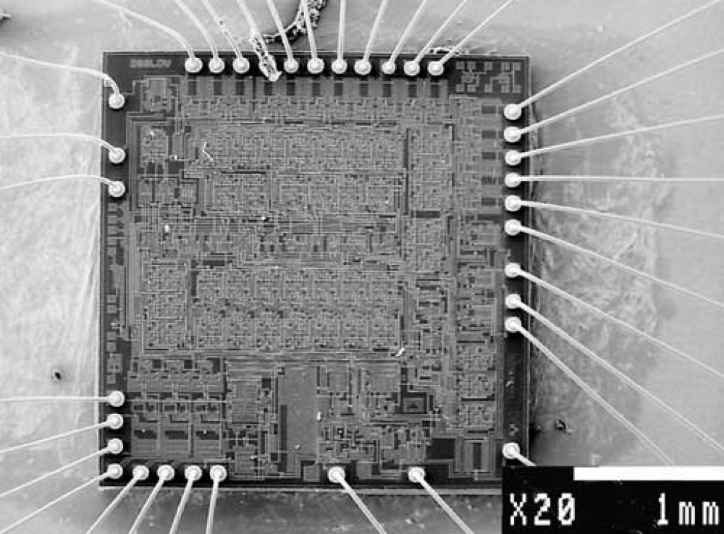
Reverse Engineering Microprocessor ATmega1284PV Embedded Firmware
We can reverse engineering Microprocessor ATMEGA1284PV embedded firmware, please view the Microprocessor ATMEGA1284PV features for your reference:
These bits select the voltage reference for the ADC, as shown in Table 19. If these bits are changed during a conversion, the change will not go into effect until this conversion is complete (ADIF in ADCSR is set).
Whenever these bits are changed, the next conversion will take 25 ADC clock cycles. If active channels are used, using AVCC or an external AREF higher than (AVCC – 1V) is not recommended, as this will affect ADC accuracy.
The internal voltage reference options may not be used if an external reference voltage is being applied to the AREF pin. The ADLAR bit affects the presentation of the ADC conversion result in the ADC Data Register.
If ADLAR is cleared, the result is right-adjusted. If ADLAR is set, the result is left-adjusted. Changing the ADLAR bit will affect the ADC Data Register immediately, regardless of any ongoing conversions after reverse engineering Microprocessor ATMEGA1284PV embedded firmware.
For a complete description of this bit, see “The ADC Data Register. The value of these bits selects which analog input is connected to the ADC. In case of differential input (PB3 – PB4), gain selection is also made with these bits. Selecting PB3 as both inputs to the differential gain stage enables offset measurements.
Refer to Table 20 for details. If these bits are changed during a conversion, the change will not go into effect until this conversion is complete (ADIF in ADCSR is set). Writing a logical “1” to this bit enables the ADC. By clearing this bit to zero, the ADC is turned off if reverse engineering Microprocessor ATMEGA1284PV embedded firmware.
Turning the ADC off while a conversion is in progress will terminate this conversion. In Single Conversion mode, a logical “1” must be written to this bit to start each conversion. In Free Running mode, a logical “1” must be written to this bit to start the first conversion.
When the conversion completes, ADSC returns to zero in Single Conversion mode and stays high in Free Running mode. Writing a “0” to this bit has no effect. When this bit is set (one), the ADC operates in Free Running mode. In this mode, the ADC samples and updates the data registers continuously after reverse engineering Microprocessor ATMEGA1284PV embedded firmware.
Clearing this bit (zero) will terminate Free Running mode. If active channels are used (MUX2 in ADMUX set), the channel must be selected before entering Free Running mode. Selecting an active channel after entering Free Running mode may result in undefined operation from the ADC when reverse engineering Microcontroller.
Brute Force Chip Break Application
Brute force chip break can be also applied to a hardware design implemented into an ASIC or a CPLD. In this case the chip breaker tries to apply all possible logic combinations to the input of the device while observing all its outputs.
That kind of microcontroller breaking could be also called black-box analysis because the MCU cracker does not have to know anything about the design of the device under test.
He only tries to understand the function of the device by trying all possible combinations of signals. This approach works well only for relatively small logic devices. Another problem the MCU reading process will face is that designs implemented in CPLDs or ASICs have flip-flops, so the output will probably be function of both the previous state and the input.
But the search space can be significantly reduced if the signals are observed and analysed beforehand. For example, clock inputs, data buses and some control signals could be easily identified, significantly reducing the area of search.