Archive for September, 2012
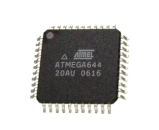
 Break IC ATmega644 Eeprom
Break IC ATmega644 Eeprom can reset the microcontroller atmega644 fuse bit by MCU unlocking skill, and extract firmware of MCU ATmega644 memory;
These bits define the division factor between the selected clock source and the internal system clock. These bits can be written run-time to vary the clock frequency to suit the application requirements. As the divider divides the master clock input to the IC, the speed of all synchronous peripherals is reduced when a division factor is used.
The division factors are given in Table 20. The CKDIV8 Fuse determines the initial value of the CLKPS bits. If CKDIV8 is uneeprommed, the CLKPS bits will be reset to “0000”. If CKDIV8 is eeprommed, CLKPS bits are reset to “0011”, giving a division factor of 8 at start up. This feature should be used if the selected clock source has a higher frequency than the maximum frequency of the device at the present operating conditions. Note that any value can be written to the CLKPS bits regardless of the CKDIV8 Fuse setting.
The Application software must ensure that a sufficient division factor is chosen if the selected clock source has a higher frequency than the maximum frequency of the device at the present operating conditions before break IC eeprom after attack microcontroller st62t15c6 firmware.
The device is shipped with the CKDIV8 Fuse eeprommed. Sleep modes enable the application to shut down unused modules in the IC, thereby saving power. The AVR provides various sleep modes allowing the user to tailor the power consumption to the application’s requirements.
To enter any of the five sleep modes, the SE bit in SMCR must be written to logic one and a SLEEP instruction must be executed. The SM2, SM1, and SM0 bits in the SMCR Register select which sleep mode (Idle, ADC Noise Reduction, Power-down, Power-save, or Standby) will be activated by the SLEEP instruction.
See Table 21 for a summary. If an enabled interrupt occurs while the IC is in a sleep mode, the IC wakes The IC is then halted for four cycles in addition to the start-up time, executes the interrupt routine, and resumes execution from the instruction following SLEEP. The contents of the Register File and SRAM are unaltered when the device wakes up from sleep. If a reset occurs during sleep mode, the IC wakes up and executes from the Reset Vector.
Figure 21 on page 39 presents the different clock systems in the ATmega644, and their distribution. The figure is helpful in selecting an appropriate sleep mode.
The SE bit must be written to logic one to make the IC enter the sleep mode when the SLEEP instruction is executed. To avoid the IC entering the sleep mode unless it is the eeprommer’s purpose, it is recommended to write the Sleep Enable (SE) bit to one just before the execution of the SLEEP instruction and to clear it immediately after waking up before BREAK IC.
Reverse Engineering Chip ATmega644A Code
Reverse Engineering Chip ATmega644A and extract microcontroller scheme to locate the security fuse bit of embedded flash, cut it off by breaking MCU technique, read processor atmega644a code and make new microprocessor cloning;
When the SM2..0 bits are written to 000, the SLEEP instruction makes the Chip enter Idle mode, stopping the CPU but allowing the SPI, USART, Analog Comparator, ADC, 2-wire Serial Interface, Timer/Counters, Watchdog, and the interrupt system to continue operating. This sleep mode basically halts clkCPU and clkFLASH, while allowing the other clocks to run. Idle mode enables the Chip to wake up from external triggered interrupts as well as internal ones like the Timer Overflow and USART Transmit Complete interrupts.
If wake-up from the Analog Comparator interrupt is not required, the Analog Comparator can be powered down by setting the ACD bit in the Analog Comparator Control and Status Register – ACSR. This will reduce power consumption in Idle mode. If the ADC is enabled, a conversion starts automatically when this mode is entered before attack mcu protection.
When the SM2..0 bits are written to 001, the SLEEP instruction makes the Chip enter ADC Noise Reduction mode, stopping the CPU but allowing the ADC, the external interrupts, 2-wire Serial Interface address match, Timer/Counter2 and the Watchdog to continue operating (if enabled). This sleep mode basically halts clkI/O, clkCPU, and clk-FLASH, while allowing the other clocks to run.
This improves the noise environment for the ADC, enabling higher resolution measurements. If the ADC is enabled, a conversion starts automatically when this mode is entered when Reverse Engineering Chip code.
Apart form the ADC Conversion Complete interrupt, only an External Reset, a Watchdog System Reset, a Watchdog interrupt, a Brown-out Reset, a 2-wire serial interface interrupt, a Timer/Counter2 interrupt, an SPM/EEPROM ready interrupt, an external level interrupt on INT7:4 or a pin change interrupt can wakeup the Chip from ADC Noise Reduction mode.
When the SM2..0 bits are written to 010, the SLEEP instruction makes the Chip enter Power-down mode. In this mode, the external Oscillator is stopped, while the external interrupts, the 2-wire Serial Interface, and the Watchdog continue operating (if enabled).
Only an External Reset, a Watchdog Reset, a Brown-out Reset, 2-wire Serial Interface address match, an external level interrupt on INT7:4, an external interrupt on INT3:0, or a pin change interrupt can wake up the Chip. This sleep mode basically halts all generated clocks, allowing operation of asynchronous modules only after Reverse Engineering MICROCONTROLLER.
Hack IC firmware
Hack IC firmware can be used for different purposes depending on the goal. Sometimes copying a profitable on-the-market product can give easy money. Larger manufacturers could consider stealing intellectual property (IP) from the device and mixing it with their own IP to disguise the theft.
Others could try to steal secrets from the device either to produce a competitive product or to steal service. Product designers should first think about the possible motives for cracking microcontroller memory their devices and then concentrate on the protection mechanisms. The following MCU IC processsor Hacking scenarios should be considered during the system design.
Failure analysis involves testing and debugging silicon chips after fabrication. Very often the chip does not function in the required way, so the manufacturer wants to investigate the problem and fix it in the next revision of the die. When a new technological process or memory type is being developed, failure analysis techniques are used to measure all the parameters and make necessary alterations in further designs. Obviously such tools should provide the ability to observe signals at any point of the chip and, if necessary, make modifications to the silicon design. From the attacker’s point of view, a perfect failure analysis tool gives the ultimate
capability to circumvent security protection. It allows connection to any point on the chip die, and lets him disable the security protection by modifying the security circuit. Fortunately, with constant technological progress resulting in a significant reduction of the transistor feature
sizes, failure analysis becomes more and more complicated and expensive. It also forces the attackers to be more and more knowledgeable and experienced. Of course, not all failure analysis techniques are useful for breaking the security of chips. For example, an attacker is not interested in cross sectioning the chip, transistor sizes, thickness of the gate oxide or metallization.
Recover MCU IC Firmware
Recover MCU IC firmware can be reversible when the device can be put back into the initial state, or irreversible with permanent changes done to the device. For example, power analysis and microprobing could make ic firmware recovery a result without harming the device itself.
Certainly microprobing will leave tamper evidence but usually that does not affect further device operation. On the contrary, fault injection and UV light MCU code reading could very likely put the device into the state where the internal registers or memory contents are changed and cannot be recovered.
In addition, UV light microcontroller unlocking leave tamper evidence as they require direct access to the chip surface.
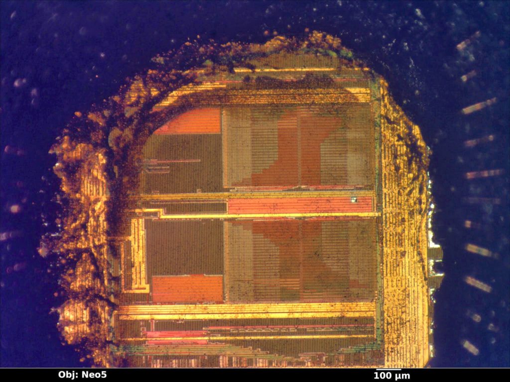
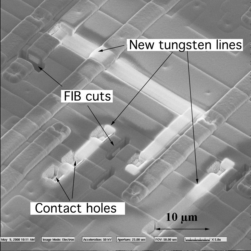
The first operation which is crucial for any invasive or semi-invasive attack is decapsulation of the chip sample to get access to the die surface. There are different techniques for doing this [66] and the most widely known and reliable method involves using hot fuming nitric acid to dissolve the plastic package material. A detailed explanation of this method is given in Chapter 5. Modern chips have multiple metal layers and in order to investigate and analyse the structure of the chip, the attacker must expose each layer, photograph it under a microscope and then combine all the photos together to get a complete picture. Then he could trace the signals from one transistor to another and simulate the whole chip. This process is called microcontroller reverse engineering and a basic overview of it is given in Chapter 5. For many years microprobing technology was used to observe the signals inside the chip during operation. This is a basic and simple way of extracting the information from semiconductor chips.
Reverse Engineering ATMEL Chip AT32UC3C264C Flash
Reverse Engineering ATMEL Chip AT32UC3C264C Flash memory’s scheme diagram and cut off the security fuse bit by MCU cracking method, focus ion beam can be applied for Microcontroller code extraction;
One 4-Channel 20-bit Pulse Width Modulation Controller (PWM)
– Complementary outputs, with Dead Time Insertion
– Output Override and Fault Protection
Two Quadrature Decoders
One 16-channel 12-bit Pipelined Analog-To-Digital Converter (ADC)
– Dual Sample and Hold Capability Allowing 2 Synchronous Conversions
– Single-Ended and Differential Channels, Window Function
Two 12-bit Digital-To-Analog Converters (DAC), with Dual Output Sample System
Four Analog Comparators
Six 16-bit Timer/Counter (TC) Channels
– External Clock Inputs, PWM, Capture and Various Counting Capabilities
One Peripheral Event Controller
– Trigger Actions in Peripherals Depending on Events Generated from Peripherals or from Input Pins
– Deterministic Trigger after samsung microcontroller S3F9454 software breaking
– 34 Events and 22 Event Actions
Five Universal Synchronous/Asynchronous Receiver/Transmitters (USART)
– Independent Baudrate Generator, Support for SPI, LIN, IrDA and ISO7816 interfaces
– Support for Hardware Handshaking, RS485 Interfaces and Modem Line
Two Master/Slave Serial Peripheral Interfaces (SPI) with Chip Select Signals
One Inter-IC Sound (I2S) Controller
– Compliant with I2S Bus Specification
– Time Division Multiplexed mode
Three Master and Three Slave Two-Wire Interfaces (TWI), 400kbit/s I2C-compatible
QTouch® Library Support
– Capacitive Touch Buttons, Sliders, and Wheels
– QTouch® and QMatrix® Acquisition
On-Chip Non-intrusive Debug System
– Nexus Class 2+, Runtime Control, Non-Intrusive Data and flash Trace
– aWire™ single-pin flashming trace and debug interface muxed with reset pin
– NanoTrace™ provides trace capabilities through JTAG or aWire interface
3 package options
– 64-pin QFN/TQFP (45 GPIO pins) package
– 100-pin TQFP (81 GPIO pins)
– 144-pin LQFP (123 GPIO pins)
Two operating voltage ranges:
– Single 5V Power Supply
– Single 3.3V Power Supply
Reverse Engineering Microcontroller AVR ATXMEGA128A1 Heximal
We can reverse engineering Microcontroller AVR ATXMEGA128A1 Heximal, please view the Microcontroller AVR ATXMEGA128A1 features for your reference:
The External Bus Interface (EBI) is the interface for connecting external peripheral and memory to the data memory space. The XMEGA A1 has 3 ports that can be used for the EBI. It can interface external SRAM, SDRAM, and/or peripherals such as LCD displays and other memory mapped devices if the heximal of microcontroller can be reverse engineeringed.
The address space, and the number of pins used, for the external memory is selectable from 256 bytes (8-bit) and up to 16M bytes (24-bit). Various multiplexing modes for address and data lines can be selected for optimal use of pins when more or less pins is available for the EBI when REVERSE ENGINEERING MICROCONTROLLER.
Each of the four chip selects has seperate configuration, and can be configured for SRAM, SRAM Low Pin Count (LPC) or SDRAM. The data memory address space associated for each chip select is decided by a configurable base address and address size for each chip celect.
For SDRAM both 4-bit SDRAM is supported, and SDRAM configurations such as CAS Latency and Refresh rate is configurable in software. The EBI is clocked from the Peripheral 2x Clock, running up to two times faster than the CPU and supporting speeds of up to 64 MHz.
The Calibration Row is a seperate memory section for factory programmed data. It contains calibration data for functions such as oscillators, device ID, and a factory programmed serial number that is unique for each device. The device ID for the available XMEGA A1 devices is shown in Table 7-1 on page 13. Some of the calibration values will be automatically loaded to the corresponding module or peripheral unit during reset. The Calibration Row can not be written or erased. It can be read from application software and external programming from reverse engineering the heximal out of microcontroller.
Break MCU Firmware
Non-invasive Break MCU Firmware are particularly dangerous in some applications for two reasons. Firstly, the owner of the device might not notice that the secret keys or data have been stolen, therefore it is unlikely that the validity of the compromised keys will be revoked before they are abused.
Secondly, non-invasive Microcontroller unlocking often scale well, as the necessary equipment can usually be reproduced and updated at low cost.
The design of most non-invasive ic cracks requires detailed knowledge of both the processor and software. On the other hand, invasive microprobing MCU reading require very little initial knowledge and usually work with a similar set of techniques on a wide range of products.
Attacks therefore often start with invasive reverse engineering, the results of which then help to develop cheaper and faster non-invasive attacks. Semi-invasive IC flash breaking can be used to learn the device functionality and test its security circuits. As these mcu cracks do not require establishing any physical contact to the internal chip layers, expensive equipment such as laser cutters and FIB machines are not required. The mcu firmware breaker could succeed using a simple off-the-shelf microscope with a photoflash or laser pointer attached to it.
Attack MCU Firmware
Attack MCU Firmware is actually a process of decapsulate the silicon package of microcontroller and disable its fuse bit by focus ion beam, then extract code from MCU flash memory;
All microprobing and reverse engineering microcontroller techniques are invasive mcu firmware attacks. They require hours or weeks in specialised laboratory and in the process they destroy the packaging.
The other three are non-invasive mcu cracking methods. The microprocessor code extracting device is not physically harmed during these ic cracks. The last MCU breaking category could also be semi-invasive. It means that the access to the chip’s die is required but the attack is not penetrative and the fault is generated with intensive light pulse, radiation, local heating or other means.
Break Chip Microprocessor ATXMEGA192A1 Eeprom
We can break Chip Microprocessor ATXMEGA192A1 Eeprom, please view the Chip Microprocessor ATXMEGA192A1 features for your reference:
The User Signature Row is a seperate memory section that is fully accessible (read and write) from application software and external programming. The User Signature Row is one flash page in size, and is meant for static user parameter storage, such as calibration data, custom serial numbers, random number seeds etc. This section is not erased by Chip Erase, and requires a dedicated erase command. This ensures parameter storage during multiple program/erase session and On-Chip Debug sessions after the eeprom of chip being break.
The Flash Program Memory and EEPROM data memory is organized in pages. The pages are word accessible for the Flash and byte accessible for the EEPROM.
Table 7-2 on page 14 shows the Flash Program Memory organization. Flash write and erase operations are performed on one page at the time, while reading the Flash is done one byte at the time. For Flash access the Z-pointer (Z[m:n]) is used for addressing.
The most significant bits in the address (FPAGE) gives the page number and the least significant address bits (FWORD) gives the word in the page. Table 7-3 on page 14 shows EEPROM memory organization for the XMEGA A1 devices.
EEPROM write and erase operations can be performed one page or one byte at the time, while reading the EEPROM is done one byte at the time. For EEPROM access the NVM Address Register (ADDR[m:n]) is used for addressing. The most significant bits in the address (E2PAGE) gives the page number and the least significant address bits (E2BYTE) gives the byte in the page before breaking eeprom of microprocessor.
Allows High-speed data transfer
– From memory to peripheral
– From memory to memory
– From peripheral to memory
– From peripheral to peripheral
4 Channels
From 1 byte and up to 16M bytes transfers in a single transaction when BREAK IC
Multiple addressing modes for source and destination address
– Increment
– Decrement
– Static
1, 2, 4, or 8 byte Burst Transfers
Programmable priority between channels
Crack MCU Firmware
The next improvement to hardware security protection was done by embedding the fuse area into the main memory array so that it shares some of the control or data lines. This implementation is more secure because the fuses are part of the memory array and their localisation is very difficult and challenging task. Fuses can share word-lines with the main memory, for example, as in the Hitachi HD6473048 microcontroller MCU;
or they can share bit-lines as in the Holtek HT48R50A microcontroller MCU. In the latter implementation the fuses do not have a separate bit-lines that for attacking MCU firmware. But that does not mean it will be more secure because the state of the fuses cannot be monitored all the time and usually is sampled at power-up and stored in a separate register.
A high level of security can be achieved if a certain memory location is used as a security fuse. In this case it would be extremely difficult to find this location and reset it without disturbing the contents of other memory cells. That does not mean that other mcu code extraction methods will not work, such as, non-invasive mcu firmware crack, but at least this reduces the chance of success with simple semi-invasive microcontroller unlocking.