Archive for July, 2012
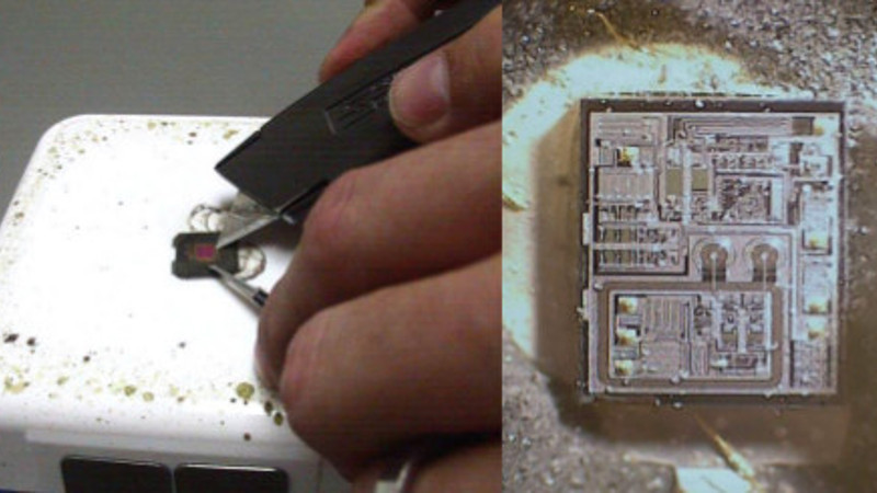
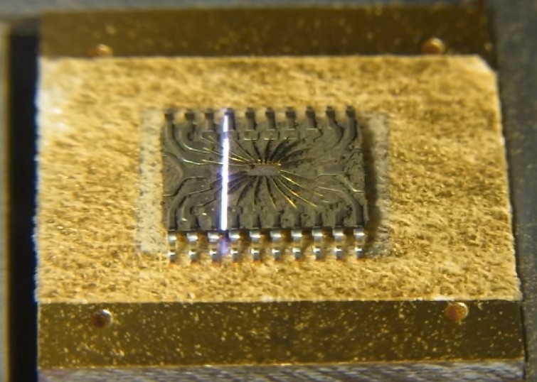
 Recovery Chip PIC16F506 Firmware
Recovery Chip PIC16F506 Firmware from microcontroller memory, crack PIC16F506 MCU flash and eeprom to readout PIC16F506 MCU code;
Random recovery operations allow the master to access any memory location in a random manner. To perform this type of recovery operation, first the word address must be set. This is done by sending the word address to the device as part of a write operation.
What sets a microcontroller apart from other processors are special circuits to deal with the needs of real-time applications. The PIC16F506 family of microcontrollers has a host of such features intended to maximize system reliability, minimize cost through elimination of external components, provide power saving operating modes and offer code protection when Reverse engineering Chip pic18f248 binary firmware.
These features are:
Oscillator selection
Reset
– Power-On Reset (POR)
– Device Reset Timer (DRT)
– Wake-up from SLEEP on pin change
Watchdog Timer (WDT)
SLEEP
Code protection
ID locations
In-circuit Serial Programming
The PIC16F506 has a Watchdog Timer which can be shut off only through configuration bit WDTE. It runs off of its own RC oscillator for added reliability.
If using XT or LP selectable oscillator options, there is always an 18 ms (nominal) delay provided by the Device Reset Timer (DRT), intended to keep the chip in reset until the crystal oscillator is stable.
If using INTRC or EXTRC there is an 18 ms delay only on VDD power-up. With this timer on-chip, most applications need no external reset circuitry.
The SLEEP mode is designed to offer a very low current power-down mode. The user can wake-up from SLEEP through a change on input pins or through a Watchdog Timer time-out. Several oscillator options are also made available to allow the part to fit the application, including an internal 4 MHz oscillator. The EXTRC oscillator option saves system cost while the LP crystal option saves power.
A set of configuration bits are used to select various options. The PIC16F506 configuration word consists of 12 bits. Configuration bits can be programmed to select various device configurations. Two bits are for the selection of the oscillator type, one bit is the Watchdog Timer enable bit, and one bit is the MCLR enable bit.
Introduction of Flexible Circuit Assembly
Flexible circuits offer some unique challenges to the assembly process. The assembly materials and processes for populating and interconnecting components to a flexible circuit range are essentially identical to those used for standard rigid or rigid flex pcb, but there are some twists required, as will be shown. The assembly processes range from very simple methods, such as manual component insertion and hand soldering (which requires little or no fixturing), to fully automated methods, which normally require specially developed, design-specific and dedicated fixtures.
How, then, does one choose an assembly process and method for flexible circuits? To begin appropriately, it is necessary to consider a number of important factors: What is the flexible circuit base material? What types of components will be used? How many assemblies will be built? These and other important questions must be addressed before one can adequately make the proper decisions regarding assembly. These seemingly simple matters can greatly influence the pcb assembly choice. For example, it is commonly assumed that polyester circuits cannot be used in applications where soldering is required. The reason for this assumption is that polyester films have a low melt point and will be grossly distorted by the tin-lead soldering process. However, when properly fixtured, soldering can be used for joining components to polyester. A number of major OEMs have been doing just that for many years. They have developed methods that provide proper shielding of the body of the polyester circuit in process. The distortion of the material can be localized to areas adjacent to the point of connection.
With the advent of the well-meant but misguided legislation mandating the use of lead-free solders, there will be significant challenges ahead, as lead-free solders have a roughly 30-40ºC higher melting temperature than traditional tin-lead solders. Sadly, it appears that traditional tin-lead solders are actually more environmentally friendly, so the law does double damage. One alternative is to use lower-temperature solders, or conductive adhesives can also be employed. The important thing is that manufacturers not limit themselves in their thinking and that they be open to alternative solutions. Following is a brief review of the key elements of flex circuit assembly.
PCB Circuit Board Electronics
Interconnect technology is expanding to include printed systems. As detailed in the iNEMI Organic and Printed Electronics Roadmap, there is a bounty of printed electronics technologies, such as “drop on demand,” Xerography, micropen, et al. It is not within the scope of this chapter to detail the principles, advantages, benefits, etc., of each technology; rather, it’s important for electronic packaging and interconnect designers to understand the salient features of printed electronics and digital fabrication technologies as well as the similarities and differences among conventional printed circuit technologies and processes.
Digital fabrication can be viewed as the creation of electro-optical-mechanical-thermal systems by means of either parallel or sequential additive processes, as controlled by a digital device. As with any technology, the designer should consider and take advantage of the technology’s features before applying it. In the case of digital fabrication, those features include adaptive, additive, roll-to-roll processes and the ability to fabricate on curved, conformal, curvilinear surfaces.
Most often, digital fabrication is accomplished in a roll-to-roll process, but panel-based digital fabrication is also possible. The revolutionary aspect of digital fabrication, as compared to conventional printed circuit board, is the ability to simultaneously create electronic and/or optical devices, electrical interconnects, mechanical structures, and thermal management systems. For example, using conventional technology and processes, a television remote control is produced by packaging and assembling tens to hundreds of electronic devices onto PCBs and subsequently assembling the PCBs, interconnect, LED, touchpad, etc., within a plastic housing. Digital fabrication would allow the entire system to be fabricated, layer-by-layer, in a fashion similar to that of stereolithography apparatus (SLA). Applying digital fabrication requires a transformation in thinking by electronic system designers: digital fabrication provides for the 2D and 3D design and fabrication of systems that are not limited to electrical interconnect and passive devices.
In digital fabrication, materials with the necessary electrical, mechanical, thermal, and optical properties to form the desired devices, systems, etc., are deposited onto a substrate. Polymer and plastic are the most common substrate materials, due to their compatibility with low-cost, high-through-put processing. However, rigid substrates can be used as well. The materials used in forming electronic devices and interconnect are, typically, conductive inks and dielectrics. Any material, however, that can be dispensed by the dispensing system (“print head” plus material control) can be used. The materials used in forming mechanical and thermal structures, likewise, are defined by the application and limited by the capabilities of the “print head” and material control system. To date, biological, organic, optical, and many types of functional materials have been printed.
Given that devices and structures are being “built-up,” layer-by-layer, there are key differences in the resulting device and feature attributes. For example, vias can be formed as filled or partially filled and can be conductive and/or nonconductive, electrically and/or thermally. Unlike conventional pcb circuit board technology and processes, digital fabrication can be used to produce vias of any geometry. Similarly, individual traces can be of any geometry and can be produced to effect sidewalls with attributes to support application needs. Conductors produced using conventional pcb manufacture technology have sidewalls that are tapered or orthogonal. Digital fabrication could be used to produce conductors with irregular sidewall features, as related to specific performance or mechanical applications. Furthermore, in digital fabrication, mechanical, thermal, and other features could be included in the construction of conductors.
Currently, the primary applications for printed electronics are OLEDs, and RFID. Photovoltaics are also an application for printed electronics, but this field is immature compared to OLEDs and RFID.
Transistors that operate in the tens of megahertz have been printed; recently, researchers at the University of Illinois (Rogers et al.) announced that they had printed silicon circuits on plastic that operate at switching speeds of 500 megahertz. As shown in Figure 27, there are demands for printed, stable, high-speed digital and high-fidelity analog devices; however, materials to produce devices other than low-speed, simple ones are lacking. Accordingly, other than novel devices produced in laboratories, printed electronics have not been used to produce the basic “building-block” high-speed digital or analog devices (e.g., FPGAs and operational amplifiers, respectively). These components are fundamental to systems comprised of analog devices.
Similarly, with respect to printing electrical interconnects, digital fabrication is in its infancy. Plated vias, a staple of the layer-to-layer interconnect found in conventional pcb circuit board technology, are nonexistent or crudely implemented in digital fabrication. Moreover, the electrical performance and reliability of vias and conductors are either not known or, with respect to characterization, known incompletely. It will be interesting to observe if and when the creation and maintenance of electronic and interconnect standards are realized.
Decrypt IC PIC16F505 Flash
Decrypt IC PIC16F505 Flash memory content, and then extract chip PIC16F505 code out and decode PIC16F505 mcu embedded firmware;
Since the device will not acknowledge during a write cycle, this can be used to determine when the cycle is complete (this feature can be used to maximize bus throughput).
Once the stop condition for a write command has been issued from the master, the device initiates the internally timed write cycle. ACK polling can be initiated immediately if break microcontroller pic12f617 binary.
This involves the master sending a start condition followed by the control byte for a write command (R/W = 0). If the device is still busy with the write cycle, then no ACK will be returned.
If no ACK is returned, then the start bit and control byte must be re-sent. If the cycle is complete, then the device will return the ACK and the master can then proceed with the next read or write command. See Figure 7-6 for flow diagram after break IC pic12hv615 heximal.
It contains an address counter that maintains the address of the last word accessed, internally incremented by one. Therefore, if the previous read access was to address n, the next current address read operation would access data from address n + 1.
Upon receipt of the slave address with the R/W bit set to one, the device issues an acknowledge and transmits the eight bit data word. The master will not acknowledge the transfer but does generate a stop condition and the device discontinues transmission.
Read operations are initiated in the same way as write operations with the exception that the R/W bit of the slave address is set to one. There are three basic types of read operations: current address read, random read and sequential read before recover mcu pic16hv616 eeprom.
Flexible Printed Circuit Board Integration
To achieve an optimal interconnect and packaging design, it is important to utilize flexible printed circuit board only when flexible printed circuit board best satisfies application and other needs.
Flexible printed circuit board is a good choice when the primary need is for flexible, conformal, thin, lightweight, etc. Flex is also a good choice for applications requiring comparatively high I/O density, low cost, or performance advantages that cannot be achieved in PCB constructions. Flexible printed circuit board can be utilized in many applications other than the aforementioned “good choices”; however, the user is strongly encouraged to consider cables, PCB, and other suitable interconnect technologies or else risk unnecessary design complexity, reliability risk, system connector challenges, higher cost, etc. As in conventional electrical design, interconnect must be partitioned according to product specifications including performance, reliability, cost, et al.
Interconnect partitioning, intentional or otherwise, can be found in the hierarchy of interconnects that is in almost any electronic system. For example, although personal computers include state-of-the-art semiconductors and their corresponding nanometer feature sizes, the power for those semiconductors is supplied through cables that are constructed using 18-gauge or larger conductors. Likewise, packaging designers need to partition the interconnect chain to satisfy system specifications, requirements, etc., using “just enough technology.”
The Flexible printed circuit board that interconnects the detector panel and signal processing electronics is a 2ML, 150-micron pitch design. One end of the Flexible printed circuit board is bonded to the panel; the other end is bonded, using ACF, to a multilayer PCB. Multiple ASICs (in bare die form) are attached, in a linear array, on the PCB; the ASICs are wirebonded to the PCB. The ASICs amplify and convert the analog signals produced by the detector panel and route those signals through a connector to a second flexible printed circuit board that connects to the system electronics. The second flexible printed circuit board, because of multiplexing of the digitized signals, requires fewer signal conductors; thus, it is a low-density 2ML flexible printed circuit board (signal plus shield layer).
The next logical step in packaging optimization for this type of electronic system would be the integration of the ASICs and ancillary electronics into the flexible printed circuit board. This integration step, if done properly, would replace the PCB with flexible printed circuit board, reduce the number of interconnects, and reduce detector panel manufacturing steps, without increasing the cost of the flex-PCB-flex system, as above.
Break IC PIC12F509 Eeprom
Break IC PIC12F509 Eeprom protection and extract hexiaml from MCU PIC12F509, reprogramme the firmware to new PIC12F509 microcontroller for cloning;
After generating a START condition, the bus master transmits a control byte consisting of a slave address and a Read/Write bit that indicates what type of operation is to be performed.
The slave address consists of a 4-bit device code (1010) followed by three don’t care bits. The last bit of the control byte determines the operation to be performed.
When set to a one a read operation is selected, and when set to a zero a write operation is selected. (Figure 7-5). The bus is monitored for its corresponding slave address all the time before recover chip pic12c508 software.
It generates an acknowledge bit if the slave address was true and it is not in a programming mode. Following the start signal from the master, the device code (4 bits), the don’t care bits (3 bits), and the R/W bit (which is a logic low) are placed onto the bus by the master transmitter.
This indicates to the addressed slave receiver that a byte with a word address will follow after it has generated an acknowledge bit during the ninth clock cycle. Therefore, the next byte transmitted by the master is the word address and will be written into the address pointer.
Only the lower four address bits are used by the device, and the upper four bits are don’t cares. The address byte is acknowledgeable and the master device will then transmit the data word to be written into the addressed memory location.
The memory acknowledges again and the master generates a stop condition. This initiates the internal write cycle, and during this time will not generate acknowledge signals. After a byte write command, the internal address counter will not be incremented and will point to the same address location that was just written.
If a stop bit is transmitted to the device at any point in the write command sequence before the entire sequence is complete, then the command will abort and no data will be written. If more than 8 data bits are transmitted before the stop bit is sent, then the device will clear the previously loaded byte and begin loading the data buffer again.
If more than one data byte is transmitted to the device and a stop bit is sent before a full eight data bits have been transmitted, then the write command will abort and no data will be written. The EEPROM memory employs a VCC threshold detector circuit which disables the internal erase/write logic if the VCC is below minimum VDD. Byte write operations must be preceded and immediately followed by a bus not busy bus cycle where both SDA and SCL are held high.
Challenge of Flexible Circuit Board
The primary challenge in today’s flexible printed circuit board technology is its I/O capability, as determined by minimum feature sizes. For example, in single-metal-layer (1ML) flexible printed circuit, trace and space widths as small as 10-microns have been produced using commercial processes, materials, etc. Even finer features have been produced, a transfer lithography process comprised of 4-micron-pitch (one-micron trace, three-micron space), flexible circuit board configuration. Similarly, feature sizes in two-metal-layer (2ML) flexible circuit board, the lion’s share of commercial flexible circuit board production, have been reduced to twenty-five microns. But minimum trace and space geometries do not tell the entire story of I/O capability for flexible circuit board.
There are many questions to pose when assessing the capabilities of potential flexible circuit board suppliers; perhaps the most critical is, what are the supplier’s minimum via land pad dimensions? The dimensions of the via land pad highlight the alignment capability of the flexible circuit board supplier’s processes and dictate the minimum pitch of the flexible circuit board interconnect. Consequently, not all 2ML flexes with twenty-five micron features have equal interconnect density. Moreover, even though feature sizes are decreasing, I/O capability in flexible circuit board is not increasing or, at a minimum, is not increasing at the same rate.
Accordingly, second-level assembly continues to move closer and closer to the device. As witnessed in chip-sized and chip-scale packages, by adapting an existing technology to a novel configuration, the unmet needs for very fine pitch, high volumetric I/O packages effected the reduction in use or elimination of standard electronic packages. Plastic encapsulated lead frames and multilayer ceramic packages have been replaced by plastic encapsulated flex interconnected bare die or, in many cases, by bare die. Similarly, the increasing use of direct chip attach results, in part, from the inability of flex interconnect to meet the constant demand for higher pixel counts in displays. In this case, package interconnect by means of wirebonds with millimeters of length and flex interconnect of tens to hundreds of millimeters in length has been replaced by stud bumps (of tens of microns in diameter, produced using the same wirebonding equipment and materials) and the complete elimination of the flex interconnect. Electronic packaging technologists and applications engineers are currently developing similar system-based solutions and applications by revisions, enhancements, etc., to existing interconnect technologies in order to meet the never-ending demand for greater interconnect density and capability. However, even though its features continue to lag behind those of semiconductors, flexible circuit board has and always will play a significant role in the optimization of system design.
Decrypt Locked Chip PIC12F508 Firmware
Decrypt Locked Chip PIC12F508 Firmware from secured program memory and data memory, microcontroller PIC12F508 cracking will help to disable the protection and readout MCU PIC12F508 heximal.
The code for these functions is available on our website www.microchip.com. The code will be accessed by either including the source code FL51XINC.ASM or by linking FLASH5IX.ASM.
It is very important to check the return codes when using these calls, and retry the operation if unsuccessful. Unsuccessful return codes occur when the EE data memory is busy with the previous write, which can take up to 4 mS if copy chip pic16c73a program.
SDA is a bi-directional pin used to transfer addresses and data into and data out of the device. For normal data transfer SDA is allowed to change only during SCL low. Changes during SCL high are reserved for indicating the START and STOP conditions.
The EEPROM interface is a 2-wire bus protocol consisting of data (SDA) and a clock (SCL). Although these lines are mapped into the GPIO register, they are not accessible as external pins; only to the internal EEPROM peripheral after recover mcu pic16f74a binary.
SDA and SCL operation is also slightly different than GPO-GP5 as listed below. Namely, to avoid code overhead in modifying the TRIS register, both SDA and SCL are always outputs.
To decrypt data from the EEPROM peripheral requires outputting a ‘1’ on SDA placing it in high-Z state, where only the internal 100K pull-up is active on the SDA line.
This code must reside in the lower half of a page. The code achieves it’s small size without additional calls through the use of a sequencing table. The table is a list of procedures that must be called in order.
The table uses an ADDWF PCL,F instruction, effectively a computed goto, to sequence to the next procedure. However the ADDWF PCL,F instruction yields an 8 bit address after recover chip pic16c71 code,
The following bus protocol is to be used with the EEPROM data memory.
Data transfer may be initiated only when the bus is not busy.
During data transfer, the data line must remain stable whenever the clock line is HIGH. Changes in the data line while the clock line is HIGH will be interpreted as a period of the clock signal. There is one bit of data per clock pulse.
Each data transfer is initiated with a START condition and terminated with a STOP condition. The number of the data bytes transferred between the START and STOP conditions is determined by the master device and is theoretically unlimited if Decrypt locked Chip Firmware. A HIGH to LOW transition of the SDA line while the clock (SCL) is HIGH determines a START condition. All commands must be preceded by a START condition. A LOW to HIGH transition of the SDA line while the clock (SCL) is HIGH determines a STOP condition. All operations must be ended with a STOP condition.
System-Based Flexible PCB Applications
The demand for thin, lightweight, high-density interconnect continues unabated. Similarly, application strategies for satisfying the ever-changing and ever-growing demand for high-density interconnect continue to change. Since their inception, flexible PCB have evolved into a cornerstone technology of high-density interconnect. Flexible PCB has become a fundamental interconnect technology, from its first application in tape automated bonding (TAB) and corresponding simple, point-to-point configurations to the fine-pitch, multilayer designs that are commonplace in today’s mobile electronic products. However, the approaches in using flexible PCB to satisfy the demands of high-performance, highly reliable systems with high volumetric density I/O are still evolving.
Following a familiar path of technology development, the use of flexible PCB has changed from first-level to second-level interconnect applications; More recently, the role of flexible PCB has been expanded to include system-level interconnect. At each point in its changing role in applications, flexible PCB technology has been modified to meet the application demands. For example, to meet the demands of die-to-die interconnect, the single-layer, via-less, point-to-point circuits found in 1970s TAB packaging sprouted additional layers. The transformation to multilayer interconnect required the development of new features such as vias for interconnecting layers; new materials such as adhesives to bond dielectric and conductor layers; and new processes and equipment for manufacturing the resulting incarnation of flexible PCB. As device I/O increased beyond the capabilities of existing multilayer technology, the trace and space features of flexible PCB were reduced. Over the past twenty years, feature sizes in flexible PCB such as conductor geometry, via diameter, dielectric thickness, etc., have been improved significantly. These improvements positioned flexible PCB for its now-dominant position in portable consumer, display, and medical electronics interconnect applications.
As witnessed over the past ten years, the reduction in interconnect feature size has slowed. At the same time, device I/O counts have increased as semiconductor features have decreased, according to Moore’s Law. This disparity in interconnect and semiconductor feature size has created an interconnect “brick wall” that demonstrates the need for advancing the capabilities of interconnect systems. Semiconductor device minimum feature size (and rate of decrease in feature size) far exceeds the equivalent in flexible PCB and PCB Clone technologies. The corresponding gap in interconnect capability has and will limit advances in semiconductor applications until advances in volumetric I/O density, form factor, weight, flexibility, etc., are implemented in flexible PCB. In the meantime, flexible PCB must be utilized as an integral part of the interconnect system.
Although the complexity of electronic systems has increased over the past ten years, the challenges in interconnect systems have been minimized due to the functional partitioning of electronic systems into key subsystems: encoding/decoding ic, processing, display, and power.
Typically, flexible PCB is utilized for interconnection within a subsystem as well as for system interconnect.
Retrieve IC PIC16LF57 Program
Retrieve IC PIC16LF57 Program from flash memory and eeprom memory, change the MCU PIC16LF57 status by unlock microcontroller‘s fuse bit and make PIC16LF57 processor copy;
The program for these functions is available on our website www.microchip.com. The program will be accessed by either including the source program FL51XINC.ASM or by linking FLASH5IX.ASM.
It is very important to check the return programs when using these calls, and retry the operation if unsuccessful. Unsuccessful return programs occur when the EE data memory is busy with the previous write, which can take up to 4 mS if break IC PIC16F884 code.
SDA is a bi-directional pin used to transfer addresses and data into and data out of the device. For normal data transfer SDA is allowed to change only during SCL low.
Changes during SCL high are reserved for indicating the START and STOP conditions. The EEPROM interface is a 2-wire bus protocol consisting of data (SDA) and a clock (SCL). Although these lines are mapped into the GPIO register, they are not accessible as external pins; only to the internal EEPROM peripheral after break IC PIC16F72A binary.
SDA and SCL operation is also slightly different than GPO-GP5 as listed below. Namely, to avoid program overhead in modifying the TRIS register, both SDA and SCL are always outputs. To read data from the EEPROM peripheral requires outputting a ‘1’ on SDA placing it in high-Z state, where only the internal 100K pull-up is active on the SDA line.
This program must reside in the lower half of a page. The program achieves it’s small size without additional calls through the use of a sequencing table. The table is a list of procedures that must be called in order. The table uses an ADDWF PCL,F instruction, effectively a computed goto, to sequence to the next procedure after Reverse eng microcontroller pic16c65b eeprom.