Archive for November, 2010
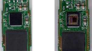
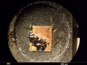
 Break Microcontroller ATmega461A Firmware
Break Microcontroller ATmega461A and readout Firmware from MCU ATmega461A flash memory, to make the MCU ATmega461A cloning;
The ATMEGA461A is a complex microcontroller with more peripheral units than can be supported within the 64 location reserved in the Opcode for the IN and OUT instructions.
For the Extended I/O space from $060 – $1FF in SRAM, only the ST/STS/STD and LD/LDS/LDD instructions can be used. The first 4,608/8,704 Data Memory locations address both the Register File, the I/O Memory, Extended I/O Memory, and the internal data SRAM if Break microcontroller attiny48v firmware.
The first 32 locations address the Register file, the next 64 location the standard I/O Memory, then 416 locations of Extended I/O memory and the next 8,192 locations address the internal data SRAM.
An optional external data SRAM can be used with the ATmega461. This SRAM will occupy an area in the remaining address locations in the 64K address space. This area starts at the address following the internal SRAM after Break IC ATtiny48A software.
The Register file, I/O, Extended I/O and Internal SRAM occupies the lowest 4,608/8,704 bytes, so when using 64KB (65,536 bytes) of External Memory, 60,478/56,832 Bytes of External Memory are available. See “External Memory Interface” on page 29 for details on how to take advantage of the external memory map.
When the addresses accessing the SRAM memory space exceeds the internal data memory locations, the external data SRAM is accessed using the same instructions as for the internal data memory access. When the internal data memories are accessed, the break and write strobe pins (PG0 and PG1) are inactive during the whole access cycle.
External SRAM operation is enabled by setting the SRE bit in the XMCRA Register. Accessing external SRAM takes one additional clock cycle per byte compared to access of the internal SRAM when recover chip atmega261a program.
This means that the commands LD, ST, LDS, STS, LDD, STD, PUSH, and POP take one additional clock cycle. If the Stack is placed in external SRAM, interrupts, subroutine calls and returns take three clock cycles extra because the three-byte program counter is pushed and popped, and external memory access does not take advantage of the internal pipe-line memory access.
When external SRAM interface is used with wait-state, one-byte external access takes two, three, or four additional clock cycles for one, two, and three wait-states respectively. Interrupts, subroutine calls and returns will need five, seven, or nine clock cycles more than specified in the instruction set manual for one, two, and three wait-states.
The five different addressing modes for the data memory cover: Direct, Indirect with Displacement, Indirect, Indirect with Pre-decrement, and Indirect with Post-increment. In the Register file, registers R26 to R31 feature the indirect addressing pointer registers.
The direct addressing reaches the entire data space. The Indirect with Displacement mode reaches 63 address locations from the base address given by the Y- or Z-register.
When using register indirect addressing modes with automatic pre-decrement and post increment, the address registers X, Y, and Z are decremented or incremented.
The 32 general purpose working registers, 64 I/O registers, and the 4,196/8,192 bytes of internal data SRAM in the ATmega640/1280/1281/2560/2561 are all accessible through all these addressing modes. The Register File is described in “General Purpose Register File” on page 12.
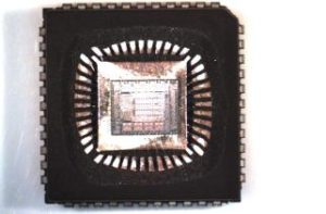
Break IC PIC16F914 Heximal
Break IC PIC16F914 is a process to crack PIC16F914 MCU protective system and then extract firmware from microcontroller PIC16F914 flash memory and eeprom memory;
Low-Power Features:
· Standby Current:
– <100 nA @ 2.0V, typical
· Operating Current:
– 11 ìA @ 32 kHz, 2.0V, typical
– 220 ìA @ 4 MHz, 2.0V, typical
· Watchdog Timer Current:
– 1 ìA @ 2.0V, typical
Peripheral Features:
· Liquid Crystal Display module:
– Up to 60/96/168 pixel drive capability on 28/40/64-pin devices, respectively
– Four commons
· Up to 24/35/53 I/O pins and 1 input-only pin:
– High-current source/sink for direct LED drive
– Interrupt-on-change pin
– Individually programmable weak pull-ups
· In-Circuit Serial Programming™ (ICSP™) via two pins
· Analog comparator module with:
– Two analog comparators
– Programmable on-chip voltage reference (CVREF) module (% of VDD) for the purpose of copying microcontroller pic16f747 code
– Comparator inputs and outputs externally accessible
· A/D Converter:
– 10-bit resolution and up to 8 channels
· Timer0: 8-bit timer/counter with 8-bit programmable prescaler
· Enhanced Timer1:
– 16-bit timer/counter with prescaler
– External Timer1 Gate (count enable)
– Option to use OSC1 and OSC2 as Timer1 oscillator if INTOSCIO or LP mode is selected
· Timer2: 8-bit timer/counter with 8-bit period register, prescaler and postscaler
· Addressable Universal Synchronous Asynchronous Receiver Transmitter (AUSART)
· Up to 2 Capture, Compare, PWM modules:
– 16-bit Capture, max. resolution 12.5 ns
– 16-bit Compare, max. resolution 200 ns
– 10-bit PWM, max. frequency 20 kHz
· Synchronous Serial Port (SSP) with I2C™
Circuit Engineering Company Limited continues to be recognized as the Southern China Leader in Services for MCU Attack, IC Break, Chip Extract, Microcontroller Unlock service. With the advancement of today’s modern circuit board technology, it is more important than ever to have specialists available to help you at a moment’s notice. Our engineering and commercial teams collectively have a vast amount of electronic experience covering field include Consumer Electronics, Industrial Automation Electronics, Wireless Communication Electronics., etc. For more information please contact us through email.
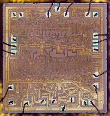
Break Chip PIC16F785 Heximal
Break Chip PIC16F785 and readout the Heximal content from MCU PIC16F785, the fuse bit of microcontroller PIC16F785 will be unlocked for opening status;
High-Performance RISC CPU:
· Only 35 Instructions to Learn:
– All single-cycle instructions except branches
· Operating Speed:
– DC – 20 MHz oscillator/clock input
– DC – 200 ns instruction cycle
· Interrupt Capability
· 8-Level Seep Hardware Stack
· Direct, Indirect and Relative Addressing modes
Special Microcontroller Features:
· Precision Internal Oscillator:
– Factory calibrated to ±1%
– Software selectable frequency range of 8 MHz to 32 kHz
– Software tunable
– Two-Speed Start-up mode
– Crystal fail detect for critical applications
– Clock mode switching during operation for power savings after recover mcu p89lpc925fdh hex
· Power-Saving Sleep mode
· Wide Operating Voltage Range (2.0V-5.5V)
· Industrial and Extended Temperature Range
· Power-on Reset (POR)
· Power-up Timer (PWRT) and Oscillator Start-up Timer (OST)
· Brown-out Reset (BOR) with Software Control Option
· Enhanced Low-Current Watchdog Timer (WDT) with on-chip Oscillator (software selectable nominal 268 seconds with full prescaler) with Software Enable
· Multiplexed Master Clear with Pull-up/Input Pin if break chip
· Programmable Code Protection
· High-Endurance Flash/EEPROM cell:
– 100,000 write Flash endurance
– 1,000,000 write EEPROM endurance
– Flash/Data EEPROM retention: > 40 years
Low-Power Features:
· Standby Current:
– 30 nA @ 2.0V, typical
· Operating Current:
– 8.5 ìA @ 32 kHz, 2.0V, typical
– 100 ìA @ 1 MHz, 2.0V, typical
· Watchdog Timer Current:
– 1 ìA @ 2.0V, typical
· Timer1 Oscillator Current:
– 2 ìA @ 32 kHz, 2.0V, typical
Peripheral Features:
· High-Speed Comparator module with:
– Two independent analog comparators
– Programmable on-chip voltage reference (CVREF) module (% of VDD) when break microcontroller pic12f629 program
– 1.2V band gap voltage reference
– Comparator inputs and outputs externally accessible
– < 40 ns propagation delay
– 2 mv offset, typical
· Operational Amplifier module with 2 independent Op Amps:
– 3 MHz GBWP, typical
– All I/O pins externally accessible
· Two-Phase Asynchronous Feedback PWM module:
– Complementary output with programmable dead band delay
– Infinite resolution analog duty cycle
– Sync Output/Input for multi-phase PWM
– FOSC/2 maximum PWM frequency
· A/D Converter:
– 10-bit resolution and 14 channels (2 internal)
· 17 I/O pins and 1 Input-only Pin:
– High-current source/sink for direct LED drive
– Interrupt-on-pin change
– Individually programmable weak pull-ups
· Timer0: 8-Bit Timer/Counter with 8-Bit Programmable Prescaler
· Enhanced Timer1:
– 16-bit timer/counter with prescaler
– External Gate Input mode
– Option to use OSC1 and OSC2 in LP mode as Timer1 oscillator, if INTOSC mode selected
· Timer2: 8-Bit Timer/Counter with 8-Bit Period Register, Prescaler and Postscaler for the purpose of break chip
· Capture, Compare, PWM module:
– 16-bit Capture, max resolution 12.5 ns
– Compare, max resolution 200 ns
– 10-bit PWM with 1 output channel, max frequency 20 kHz
· In-Circuit Serial ProgrammingTM (ICSPTM) via two pins
· Shunt Voltage Regulator (PIC16HV785 only):
– 5 volt regulation
– 4 mA to 50 mA shunt range
Copy Chip PIC16F777 Firmware
Copy Chip PIC16F777 Firmware from secured flash and eeprom memory, after crack PIC16F777 mcu security fuse bit and readout the firmware from microcontroller PIC16F777 program and data memory;
Copy Chip PIC16F777 Firmware
Status Register:
The Status register contains the arithmetic status of the ALU, the Reset status and the bank select bits for data memory
The Status register can be the destination for any instruction, as with any other register. If the Status register is the destination for an instruction that affects the Z, DC or C bits, then the write to these three bits is disabled. These bits are set or cleared according to the device logic.
Furthermore, the TO and PD bits are not writable, therefore, the result of an instruction with the Status register as destination may be different than intended.
For example, CLRF STATUS, will clear the upper three bits and set the Z bit. This leaves the Status register as 000u u1uu (where u = unchanged).
It is recommended, therefore, that only BCF, BSF, SWAPF and MOVWF instructions are used to alter the Status register because these instructions do not affect the Z, C or DC bits from the Status register. For other instructions not affecting any Status bits e, the result of an instruction with the Status register as destination may be different than intended after Copy Chip pic16f886 firmware.
The Program Counter (PC) is 13 bits wide. The low byte comes from the PCL register which is a readable and writable register. The upper bits (PC<12:8>) are not readable but are indirectly writable through the PCLATH register. On any Reset, the upper bits of the PC will be cleared. Figure 2-4 shows the two situations for the loading of the PC. The upper example in the figure shows how the PC is loaded on a write to PCL (PCLATH<4:0> → PCH). The lower example in the figure shows how the PC is loaded during a CALL or GOTO instruction (PCLATH<4:3> → PCH) for the purpose of Copy mcu at89c55wd bin.
The stack operates as a circular buffer. This means that after the stack has been PUSHed eight times, the ninth push overwrites the value that was stored from the first push. The tenth push overwrites the second push (and so on).
PIC16F7X7 devices are capable of addressing a con- been PUSHed eight times, the ninth push overwrites the value that was stored from the first push. The tenth push overwrites the second push (and so on). tinuous 8K word block of program memory. The CALL and GOTO instructions provide only 11 bits of address to allow branching within any 2K program memory page.
When doing a CALL or GOTO instruction, the upper 2 bits of the address are provided by PCLATH<4:3>.
Copy Microcontroller PIC16F767 Program
Copy Microcontroller PIC16F767 Program from embedded program memory, protection of mcu pic16f767 will be attacked and copy the new firmware into new MCU pic16f767;
Copy Microcontroller PIC16F767 Program from embedded program memory, protection of mcu pic16f767 will be attacked and copy the new firmware into new MCU pic16f767
MEMORY ORGANIZATION
There are two memory blocks in each of these PICmicro® MCUs. The program memory and data memory have separate buses so that concurrent access can occur and is detailed in this section. The program memory can be read internally by user code (see Section 3.0 “Reading Program Memory”) when copy P87C51X2BBD microcontroller.
Additional information on device memory may be found in the “PICmicro® Mid-Range MCU Family Reference Manual” (DS33023).
The PIC16F767 devices have a 13-bit program counter capable of addressing an 8K word x 14-bit program memory space. The PIC16F767 devices have 8K words of Flash program memory and the PIC16F767 devices have 4K words. The program memory maps for PIC16F7X7 devices are shown in Figure 2-1. Accessing a location above the physically implemented address will cause a wraparound. in the “PICmicro® Mid-Range MCU Family Reference.
The Reset vector is at 0000h and the interrupt vector is at 0004h.
The data memory is partitioned into multiple banks which contain the General Purpose Registers and the Special Function Registers. Bits RP1 (Status<6>) and RP0 (Status<5>) are the bank select bits if copy recover 430G2452 microcontroller:
Each bank extends up to 7Fh (128 bytes). The lower locations of each bank are reserved for the Special Function Registers. Above the Special Function Registers are General Purpose Registers, implemented as static RAM. All implemented banks contain Special Function Registers. Some frequently used Special Function Registers from one bank may be mirrored in another bank for code reduction and quicker access.
Copy Microcontroller PIC16F747 Code
Copy Microcontroller PIC16F747 Code from embedded flash and eeprom memory, and extract the firmware from MCU pic16f747 memory after crack MCU protection;
Copy Microcontroller PIC16F747 Code from embedded flash and eeprom memory, and extract the firmware from MCU pic16f747 memory after crack MCU protection
Special Microcontroller Features:
· Fail-Safe Clock Monitor for protecting critical applications against crystal failure;
· Two-Speed Start-up mode for immediate code execution
· Power-on Reset (POR), Power-up Timer (PWRT) and Oscillator Start-up Timer (OST)
· Programmable Code Protection
· Processor Read Access to Program Memory
· Power-Saving Sleep mode
· In-Circuit Serial Programming (ICSP) via two pins
· MPLAB® In-Circuit Debug (ICD) via two pins
· MCLR pin function replaceable with input only pin if Copy chip pic16f870 program
DEVICE OVERVIEW
This document contains device specific information about the following devices:
PIC16F737/767 devices are available only in 28-pin packages, while PIC16F747/777 devices are available in 40-pin and 44-pin packages. All devices in the PIC16F7X7 family share common architecture with the following differences:
· The PIC16F737 and PIC16F767 have one-half of the total on-chip memory of the PIC16F747 and PIC16F777.
· The 28-pin devices have 3 I/O ports, while the 40/44-pin devices have 5.
· The 28-pin devices have 16 interrupts, while the 40/44-pin devices have 17.
· The 28-pin devices have 11 A/D input channels, while the 40/44-pin devices have 14.
· The Parallel Slave Port is implemented only on the 40/44-pin devices.
· Low-Power modes: RC_RUN allows the core and peripherals to be clocked from the INTRC, while SEC_RUN allows the core and peripherals to be clocked from the low-power Timer1. Refer to
Section 4.7 “Power-Managed Modes” for further details for the purpose of break pic18f8722 Microcontroller code.
· Internal RC oscillator with eight selectable frequencies, including 31.25 kHz, 125 kHz, 250 kHz, 500 kHz, 1 MHz, 2 MHz, 4 MHz and 8 MHz. The INTRC can be configured as a primary or secondary clock source. Refer to Section 4.5 “Internal Oscillator Block” for further details.
Recover Chip ATmega261A Program
Recover Chip ATmega261A means the program of MCU ATmega261A from flash memory and eeprom memory will be readout and fuse bit of Microcontroller ATmega261A will be unlocked;
There are basically two types of interrupts. The first type is triggered by an event that sets the Interrupt Flag. For these interrupts, the Program Counter is vectored to the actual Interrupt Vector in order to execute the interrupt handling routine, and hardware clears the corresponding Interrupt Flag.
Interrupt Flags can also be cleared by writing a logic one to the flag bit position(s) to be cleared. If an interrupt condition occurs while the corresponding interrupt enable bit is cleared, the Interrupt Flag will be set and remembered until the interrupt is enabled, or the flag is cleared by software if break mcu atmega64pa binary.
Similarly, if one or more interrupt conditions occur while the Global Interrupt Enable bit is cleared, the corresponding Interrupt Flag(s) will be set and remembered until the Global Interrupt Enable bit is set, and will then be executed by order of priority.
The second type of interrupts will trigger as long as the interrupt condition is present. These interrupts do not necessarily have Interrupt Flags. If the interrupt condition disappears before the interrupt is enabled, the interrupt will not be triggered after break ic atmega128a firmware.
When the AVR exits from an interrupt, it will always return to the main program and execute one more instruction before any pending interrupt is served. Note that the Status Register is not automatChipally stored when entering an interrupt routine, nor restored when returning from an interrupt routine.
This must be handled by software. When using the CLI instruction to disable interrupts, the interrupts will be immediately disabled. No interrupt will be executed after the CLI instruction, even if it occurs simultaneously with the CLI instruction. The following example shows how this can be used to avoid interrupts during the timed EEPROM write sequence.
The interrupt execution response for all the enabled AVR interrupts is five clock cycles minimum. After five clock cycles the program vector address for the actual interrupt handling routine is executed. During these five clock cycle period, the Program Counter is pushed onto the Stack when Recover ic atmega168pa program.
The vector is normally a jump to the interrupt routine, and this jump takes three clock cycles. If an interrupt occurs during execution of a multi-cycle instruction, this instruction is completed before the interrupt is served.
If an interrupt occurs when the MCU is in sleep mode, the interrupt execution response time is increased by five clock cycles. This increase comes in addition to the start-up time from the selected sleep mode.
A return from an interrupt handling routine takes five clock cycles. During these five clock cycles, the Program Counter (three bytes) is popped back from the Stack, the Stack Pointer is incremented by three, and the I-bit in SREG is set.