Archive for May, 2010
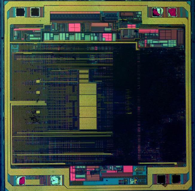
 Break Chip ATmega162L Firmware
Break Chip ATmega162L and extract mcu atmega162 memory firmware, copy avr atmega162 flash memory content to new mcu atmega162;
If 9-bit characters are used (UCSZn=7) the ninth bit must be break from the RXB8n bit in UCSRnB before breaking the low bits from the UDRn. This rule applies to the FEn, DORn and UPEn Status Flags as well.
Break status from UCSRnA, then data from UDRn. Breaking the UDRn I/O location will change the state of the receive buffer FIFO and consequently the TXB8n, FEn, DORn and UPEn bits, which all are stored in the FIFO, will change if recover microprocessor atmega1281pa flash memory.
The following Firmware example shows a simple USART receive function that handles both nine bit characters and the status bits.
The receive function example breaks all the I/O Registers into the Register File before any computation is done. This gives an optimal receive buffer utilization since the buffer location break will be free to accept new data as early as possible after Break MCU ATmega2560pa hex.
The USART Receiver has one flag that indicates the Receiver state. The Receive Complete (RXCn) Flag indicates if there are unbreak data present in the receive buffer.
This flag is one when unbreak data exist in the receive buffer, and zero when the receive buffer is empty (i.e., does not contain any unbreak data). If the Receiver is disabled (RXENn = 0), the receive buffer will be flushed and consequently the RXCn bit will become zero.
When the Receive Complete Interrupt Enable (RXCIEn) in UCSRnB is set, the USART Receive Complete interrupt will be executed as long as the RXCn Flag is set (provided that global interrupts are enabled).
When interrupt-driven data reception is used, the receive complete routine must break the received data from UDRn in order to clear the RXCn Flag, otherwise a new interrupt will occur once the interrupt routine terminates.
Break MCU PIC18F442 Software
Break MCU PIC18F442 and extract embedded code from microcontroller pic18f442, the encrypted flash memory heximal of microprocessor pic18f442 will be unlocked;

The top of the stack is breakable and writable. Three register locations, TOSU, TOSH and TOSL hold the contents of the stack location pointed to by the STKPTR register. This allows users to implement a software stack if necessary.
After a CALL, RCALL or interrupt, the software can break the pushed value by breaking the TOSU, TOSH and TOSL registers. These values can be placed on a user defined software stack when Break pic16f88 Mcu data.
At return time, the software can replace the TOSU, TOSH and TOSL and do a return. The user must disable the global interrupt enable bits during this time to prevent inadvertent stack operations.
The STKPTR register contains the stack pointer value, the STKFUL (stack full) status bit, and the STKUNF (stack underflow) status bits. Register 4-1 shows the STKPTR register. The value of the stack pointer can be 0 through 31. The stack pointer increments when values are pushed onto the stack and decrements when values are popped off the stack. At RESET, the stack pointer value will be used to Breaking pic12ce518 Mcu.
The user may break and write the stack pointer value. This feature can be used by a Real Time Operating System for return stack maintenance. After the PC is pushed onto the stack 31 times (without popping any values off the stack), the STKFUL bit is set. The STKFUL bit can only be cleared in software or by a POR.
The action that takes place when the stack becomes full depends on the state of the STVREN (Stack Over-flow Reset Enable) configuration bit. Refer to Section 20.0 for a description of the device configuration bits.
If STVREN is set (default), the 31st push will push the (PC + 2) value onto the stack, set the STKFUL bit, and reset the device. The STKFUL bit will remain set and the stack pointer will be set to ‘0’.
If STVREN is cleared, the STKFUL bit will be set on the 31st push and the stack pointer will increment to 31. Any additional pushes will not overwrite the 31st push, and STKPTR will remain at 31.
Since the Top-of-Stack (TOS) is breakable and writable, the ability to push values onto the stack and pull values off the stack without disturbing normal program execution is a desirable option. To push the current PC value onto the stack, a PUSH instruction can be executed.
This will increment the stack pointer and load the current PC value onto the stack. TOSU, TOSH and TOSL can then be modified to place a return address on the stack.
The ability to pull the TOS value off of the stack and replace it with the value that was previously pushed onto the stack, without disturbing normal execution, is achieved by using the POP instruction. ThePOP instruction discards the current TOS by decrementing the stack pointer.
The previous value pushed onto the stack then becomes the TOS value. These resets are enabled by programming the STVREN configuration bit. When the STVREN bit is disabled, a full or underflow condition will set the appropriate STKFUL or STKUNF bit, but not cause a device RESET.
When the STVREN bit is enabled, a full or underflow will set the appropriate STKFUL or STKUNF bit and then cause a device RESET. The STKFUL or STKUNF bits are only cleared by the user software or a POR Reset.
Recover Microcontroller PIC18F252 Program
Recover Microcontroller PIC18F252 Program means the embedded heximal of mcu pic18f252 will be copied out from original flash memory after cracking protected mcu pic18f252.
Recover Microcontroller PIC18F252 Program means the embedded heximal of mcu pic18f252 will be copied out from original flash memory after cracking protected mcu pic18f252
CMOS Technology:
· Low power, high speed FLASH/EEPROM technology
· Fully static design
· Wide operating voltage range (2.0V to 5.5V)
· Industrial and Extended temperature ranges
· Low power consumption:
– < 1.6 mA typical @ 5V, 4 MHz
– 25 ìA typical @ 3V, 32 kHz
– < 0.2 ìA typical standby current
For timing-insensitive applications, the “RC” and “RCIO” device options offer additional cost savings.
The RC oscillator frequency is a function of the supply voltage, the resistor (REXT) and capacitor (CEXT) values and the operating temperature. In addition to this, the oscillator frequency will vary from unit to unit due to normal process parameter variation before copying pic16f627a microcontroller.
Furthermore, the difference in lead frame capacitance between package types will also affect the oscillation frequency, especially for low CEXT values. The user also needs to take into account variation due to tolerance of external R and C components used. Figure 2-3 shows how the R/C combination is connected.
In the RC Oscillator mode, the oscillator frequency divided by 4 is available on the OSC2 pin. This signal may be used for test purposes or to synchronize other logic.
The RCIO Oscillator mode functions like the RC mode, except that the OSC2 pin becomes an additional general purpose I/O pin. The I/O pin becomes bit 6 of PORTA (RA6).
The EC and ECIO Oscillator modes require an external clock source to be connected to the OSC1 pin. The feedback device between OSC1 and OSC2 is turned off in these modes to save current. There is no oscillator start-up time required after a Power-on Reset or after a recovery from SLEEP mode.
In the EC Oscillator mode, the oscillator frequency divided by 4 is available on the OSC2 pin. This signal may be used for test purposes or to synchronize other logic. Figure 2-4 shows the pin connections for the EC Oscillator mode.
Break IC PIC18F242 Software
Break IC PIC18F242 Software is a process to unlock encrypted mcu pic18f242 protection and open locked microcontroller pic18f242 flash memory silicon package;
Break IC PIC18F242 Software is a process to unlock encrypted mcu pic18f242 protection and open locked microcontroller pic18f242 flash memory silicon package
High Performance RISC CPU:
· C compiler optimized architecture/instruction set
– Source code compatible with the PIC16 and PIC17 instruction sets
· Linear program memory addressing to 32 Kbytes
· Linear data memory addressing to 1.5 Kbytes
· Up to 10 MIPs operation:
– DC – 40 MHz osc./clock input
– 4 MHz – 10 MHz osc./clock input with PLL active
· 16-bit wide instructions, 8-bit wide data path
· Priority levels for interrupts
· 8 x 8 Single Cycle Hardware Multiplier
Peripheral Features:
· High current sink/source 25 mA/25 mA
· Three external interrupt pins
· Timer0 module: 8-bit/16-bit timer/counter with 8-bit programmable prescaler
· Timer1 module: 16-bit timer/counter
· Timer2 module: 8-bit timer/counter with 8-bit period register (time-base for PWM)
· Timer3 module: 16-bit timer/counter
· Secondary oscillator clock option – Timer1/Timer3
· Two Capture/Compare/PWM (CCP) modules. CCP pins that can be configured as:
– Capture input: capture is 16-bit, max. resolution 6.25 ns (TCY/16)
– Compare is 16-bit, max. resolution 100 ns (TCY)
– PWM output: PWM resolution is 1- to 10-bit, max. PWM freq. @: 8-bit resolution = 156 kHz 10-bit resolution = 39 kHz
· Master Synchronous Serial Port (MSSP) module,
Two modes of operation:
– 3-wire SPI™ (supports all 4 SPI modes)
– I2C™ Master and Slave mode
Peripheral Features (Continued):
· Addressable USART module:
– Supports RS-485 and RS-232
· Parallel Slave Port (PSP) module
Analog Features:
· Compatible 10-bit Analog-to-Digital Converter module (A/D):
– Fast sampling rate
– Conversion available during SLEEP
– Linearity ≤ 1 LSb
· Programmable Low Voltage Detection (PLVD)
– Supports interrupt on-Low Voltage Detection
· Programmable Brown-out Reset (BOR)
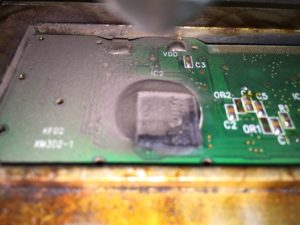
Reverse Chip ATmega162PV Heximal
Reverse Chip ATmega162PV Heximal is a process to crack microcontroller atmega162pv security fuse bit and then readout the program from mcu atmega162pv flash memory and eeprom memory;
The Parity Generator calculates the parity bit for the serial frame data. When parity bit is enabled (UPMn1 = 1), the transmitter control logic inserts the parity bit between the last data bit and the first stop bit of the frame that is sent.
The disabling of the Transmitter (setting the TXEN to zero) will not become effective until ongoing and pending transmissions are completed, i.e., when the Transmit Shift Register and Transmit Buffer Register do not contain data to be transmitted if Recover microprocessor atmega1280pa flash memory.
When disabled, the Transmitter will no longer override the TxDn pin. The USART Receiver is enabled by writing the Receive Enable (RXENn) bit in the UCSRnB Register to one.
When the Receiver is enabled, the normal pin operation of the RxDn pin is overridden by the USART and given the function as the Receiver’s serial input. The baud rate, mode of operation and frame format must be set up once before any serial reception can be done. If synchronous operation is used, the clock on the XCKn pin will be used as transfer clock when Reverse engineering mcu atmega48pv code.
The Receiver starts data reception when it detects a valid start bit. Each bit that follows the start bit will be sampled at the baud rate or XCKn clock, and shifted into the Receive Shift Register until the first stop bit of a frame is received.
A second stop bit will be ignored by the Receiver. When the first stop bit is received, i.e., a complete serial frame is present in the Receive Shift Register, the contents of the Shift Register will be moved into the receive buffer.
The receive buffer can then be reverse by reverseing the UDRn I/O location. The following code example shows a simple USART receive function based on polling of the Receive Complete (RXCn) Flag after Recover atmega88pv Chip firmware.
When using frames with less than eight bits the most significant bits of the data reverse from the UDRn will be masked to zero. The USART has to be initialized before the function can be used.
Recover MCU PIC16HV616 Eeprom
Recover MCU PIC16HV616 Eeprom content needs to crack microcomputer chip pic16hv616 and readout the embedded heximal from microcontroller pic16hv616 flash memory;
The data memory (see Figure 2-4) is partitioned into two banks, which contain the General Purpose Registers (GPR) and the Special Function Registers (SFR). The Special Function Registers are located in the first 32 locations of each bank.
PIC16F610/16HV610 Register locations 40h-7Fh in Bank 0 are General Purpose Registers, implemented as static RAM. PIC16F616/16HV616 Register locations 20h-7Fh in Bank 0 and A0h-BFh in Bank 1 are General Purpose Registers, implemented as static RAM. Register locations F0h-FFh in Bank 1 point to addresses 70h-7Fh in Bank 0. All other RAM is unimplemented and returns ‘0’ when read. The RP0 bit of the STATUS register is the bank select bit.
The register file is organized as 64 x 8 in the PIC16F610/16HV610 and 128 x 8 in the PIC16F616/16HV616. Each register is accessed, either directly or indirectly, through the File Select Register (FSR) (see Section 2.4 “Indirect Addressing, INDF and FSR Registers”) if copy pic16c72 Mcu software.
The Special Function Registers are registers used by the CPU and peripheral functions for controlling the desired operation of the device (see Table 2-1). These registers are static RAM. The special registers can be classified into two sets: core and peripheral. The Special Function Registers associated with the “core” are described in this section. Those related to the operation of the peripheral features are described in the section of that peripheral feature.
The STATUS register, shown in Register 2-1, contains:
· the arithmetic status of the ALU
· the Reset status
· the bank select bits for data memory (RAM)
The STATUS register can be the destination for any instruction, like any other register. If the STATUS register is the destination for an instruction that affects the Z, DC or C bits, then the write to these three bits is disabled. These bits are set or cleared according to the device logic. Furthermore, the TO and PD bits are not writable. Therefore, the result of an instruction with the STATUS register as destination may be different than intended.
For example, CLRF STATUS, will clear the upper three bits and set the Z bit. This leaves the STATUS register as ‘000u u1uu’ (where u = unchanged). The Program Counter (PC) is 13 bits wide. The low byte comes from the PCL register, which is a readable and writable register. The high byte (PC<12:8>) is not directly readable or writable and comes from PCLATH. On any Reset, the PC is cleared.
Figure 2-5 shows the two situations for the loading of the PC. The upper example in Figure 2-5 shows how the PC is loaded on a write to PCL (PCLATH<4:0> → PCH). The lower example in Figure 2-5 shows how the PC is loaded during aCALL or GOTO instruction (PCLATH<4:3> → PCH).
Recover IC ATmega162PA Binary
Recover IC ATmega162PA Binary from locked memory which include flash and eeprom, extract the code from mcu atmega162pa and copy heximal to new microcontroller atmega162pa;
The USART has to be initialized before any communication can take place. The initialization process normally consists of setting the baud rate, setting frame format and enabling the Transmitter or the Receiver depending on the usage.
For interrupt driven USART operation, the Global Interrupt Flag should be cleared (and interrupts globally disabled) when doing the initialization if Reverse mcu atmega461pv IC binary.
Before doing a re-initialization with changed baud rate or frame format, be sure that there are no ongoing transmissions during the period the registers are changed. The TXCn Flag can be used to check that the Transmitter has completed all transfers, an the RXC Flag can be used to check that there are no unread data in the receive buffer.
Note that the TXCn Flag must be cleared before each transmission (before UDRn is written) if it is used for this purpose. The following simple USART initialization binary examples show one assembly and one C function that are equal in functionality.
The examples assume asynchronous operation using polling (no interrupts enabled) and a fixed frame format. The baud rate is given as a function parameter. For the assembly binary, the baud rate parameter is assumed to be stored in the r17:r16 Registers after Reverse microcontroller atmega8p archive.
More advanced initialization routines can be made that include frame format as parameters, disable interrupts and so on. However, many applications use a fixed setting of the baud and control registers, and for these types of applications the initialization binary can be placed directly in the main routine, or be combined with initialization binary for other I/O modules.
The USART Transmitter is enabled by setting the Transmit Enable (TXEN) bit in the UCSRnB Register. When the Transmitter is enabled, the normal port operation of the TxDn pin is overridden by the USART and given the function as the Transmitter’s serial output.
The baud rate, mode of operation and frame format must be set up once before doing any transmissions. If synchronous operation is used, the clock on the XCKn pin will be overridden and used as transmission clock.
Reverse Engineering Microcontroller PIC16HV610 Program
Reverse Engineering Microcontroller PIC16HV610 is a process to locate the fuse bit of mcu and unlock pic16hv610 protection, extract mcu code from pic16hv610 memory;
Reverse Engineering Microcontroller PIC16HV610 Program
We can Reverse engineering Microcontroller PIC16HV610 Program, please view the Microcontroller PIC16HV610 features for your reference:
High-Performance RISC CPU:
· Only 35 instructions to learn:
– All single-cycle instructions except branches
· Operating speed:
– DC – 20 MHz oscillator/clock input
– DC – 200 ns instruction cycle
· Interrupt capability
· 8-level deep hardware stack
· Direct, Indirect and Relative Addressing modes
Special Microcontroller Features:
· Precision Internal Oscillator:
– Factory calibrated to ±1%, typical
– User selectable frequency: 4 MHz or 8 MHz
· Power-Saving Sleep mode
· Voltage range:
– PIC16F610/616: 2.0V to 5.5V
– PIC16HV610/616: 2.0V to user defined maximum (see note)
· Industrial and Extended Temperature range
· Power-on Reset (POR)
· Power-up Timer (PWRT) and Oscillator Start-up Timer (OST)
· Brown-out Reset (BOR)
· Watchdog Timer (WDT) with independent oscillator for reliable operation before Reverse engineering Microcontroller
· Multiplexed Master Clear with pull-up/input pin
· Programmable code protection
· High Endurance Flash:
– 100,000 write Flash endurance
– Flash retention: > 40 years
Low-Power Features:
· Standby Current:
– 50 nA @ 2.0V, typical
· Operating Current:
– 20 ìA @ 32 kHz, 2.0V, typical
– 220 ìA @ 4 MHz, 2.0V, typical
· Watchdog Timer Current:
– 1 ìA @ 2.0V, typical
Peripheral Features:
· Shunt Voltage Regulator (PIC16HV610/616 only):
– 5 volt regulation
– 4 mA to 50 mA shunt range
· 11 I/O pins and 1 input only
– High current source/sink for direct LED drive
– Interrupt-on-Change pins
– Individually programmable weak pull-ups
· Analog Comparator module with:
– Two analog comparators
– Programmable on-chip voltage reference (CVREF) module (% of VDD)
– Fixed Voltage Reference
– Comparator inputs and outputs externally accessible
– SR Latch
– Built-In Hysteresis (user selectable)
· Timer0: 8-bit timer/counter with 8-bit programmable prescaler
· Enhanced Timer1:
– 16-bit timer/counter with prescaler
– External Timer1 Gate (count enable)
– Option to use OSC1 and OSC2 in LP mode as Timer1 oscillator if INTOSC mode selected
– Timer1 oscillator
· In-Circuit Serial ProgrammingTM (ICSPTM) via two pins
PIC16F616/16HV616 only:
· A/D Converter:
– 10-bit resolution
– 8 external input channels
– 2 internal reference channels
· Timer2: 8-bit timer/counter with 8-bit period register, prescaler and postscaler
· Enhanced Capture, Compare, PWM module:
– 16-bit Capture, max. resolution 12.5 ns
– 16-bit Compare, max. resolution 200 ns
– 10-bit PWM with 1, 2 or 4 output channels, programmable “dead time”, max. frequency 20 kHz
Break MCU ATmega162A Heximal
Break MCU ATmega162A and read microcontroller atmega162a memory content out from its secured flash memory, copy Heximal to new atmega162a processor as cloning;
The UCPOLn bit UCRSC selects which XCKn clock edge is used for data sampling and which is used for data change. As Figure 85 shows, when UCPOLn is zero the data will be changed at rising XCKn edge and sampled at falling XCKn edge.
If UCPOLn is set, the data will be changed at falling XCKn edge and sampled at rising XCKn edge. A serial frame is defined to be one character of data bits with synchronization bits (start and stop bits), and optionally a parity bit for error checking. The USART accepts all 30 combinations of the following as valid frame formats if recover microprocessor atmega1281pa flash memory:
1 start bit
5, 6, 7, 8, or 9 data bits
no, even or odd parity bit
1 or 2 stop bits
A frame starts with the start bit followed by the least significant data bit. Then the next data bits, up to a total of nine, are succeeding, ending with the most significant bit. If enabled, the parity bit is inserted after the data bits, before the stop bits.
When a complete frame is transmitted, it can be directly followed by a new frame, or the communication line can be set to an idle (high) state. Figure 86 illustrates the possible combinations of the frame formats. Bits inside brackets are optional.
The frame format used by the USART is set by the UCSZn2:0, UPMn1:0 and USBSn bits in UCSRnB and UCSRnC. The Receiver and Transmitter use the same setting when Break MCU ATmega2560pa heximal.
Note that changing the setting of any of these bits will corrupt all ongoing communication for both the Receiver and Transmitter.
The USART Character SiZe (UCSZn2:0) bits select the number of data bits in the frame. The USART Parity mode (UPMn1:0) bits enable and set the type of parity bit. The selection between one or two stop bits is done by the USART Stop Bit Select (USBSn) bit.
The Receiver ignores the second stop bit. An FE (Frame Error) will therefore only be detected in the cases where the first stop bit is zero. The parity bit is calculated by doing an exclusive-or of all the data bits. If odd parity is used, the result of the exclusive or is inverted. The relation between the parity bit and data bits.
If used, the parity bit is located between the last data bit and first stop bit of a serial frame.
Reverse IC ATmega162P Eeprom
Reverse IC ATmega162P Eeprom after crack microcontroller atmega162p protective system, and extract locked code from mcu atmega162p flash memory;
Internal clock generation is used for the asynchronous and the synchronous master modes of operation. The description in this section refers to Figure 84. The USART Baud Rate Register (UBRRn) and the down-counter connected to it function as a programmable prescaler or baud rate generator.
The down-counter, running at system clock (fosc), is loaded with the UBRRn value each time the counter has counted down to zero or when the UBRRLn Register is written. A clock is generated each time the counter reaches zero. This clock is the baud rate generator clock output (= fosc/(UBRRn+1)). The Transmitter divides the baud rate generator clock output by 2, 8 or 16 depending on mode. The baud rate generator output is used directly by the Receiver’s clock and data recovery units after Reverse IC eeprom.
However, the recovery units use a state machine that uses 2, 8 or 16 states depending on mode set by the state of the UMSELn, U2Xn and DDR_XCKn bits. Table 98 contains equations for calculating the baud rate (in bits per second) and for calculating the UBRRn value for each mode of operation using an internally generated clock source after reverse Ic eeprom.
The transfer rate can be doubled by setting the U2Xn bit in UCSRnA. Setting this bit only has effect for the asynchronous operation. Set this bit to zero when using synchronous operation if reverse ic eeprom.
Setting this bit will reduce the divisor of the baud rate divider from 16 to 8, effectively doubling the transfer rate for asynchronous communication. Note however that the Receiver will in this case only use half the number of samples (reduced from 16 to 8) for data sampling and clock recovery, and therefore a more accurate baud rate setting and system clock are required when this mode is used. For the Transmitter, there are no downsides after Reverse IC eeprom.
External clocking is used by the synchronous slave modes of operation. The description in this section refers to Figure 84 for details. External clock input from the XCKn pin is sampled by a synchronization register to minimize the chance of meta-stability. The output from the synchronization register must then pass through an edge detector before it can be used by the Transmitter and Receiver when Reverse IC eeprom.
This process introduces a two CPU clock period delay and therefore the maximum external XCKn clock frequency is limited by the following equation when Reverse IC eeprom:
Note that fosc depends on the stability of the system clock source. It is therefore recommended to add some margin to avoid possible loss of data due to frequency variations.
When synchronous mode is used (UMSELn = 1), the XCKn pin will be used as either clock input (Slave) or clock output (Master). The dependency between the clock edges and data sampling or data change is the same. The basic principle is that data input (on RxDn) is sampled at the opposite XCKn clock edge of the edge the data output (TxDn) is changed when Reverse IC eeprom.